錚?/div>
Family
Operates From 1.65 V to 3.6 V
Inputs Accept Voltages to 5.5 V
Max t
pd
of 4.4 ns at 3.3 V
Typical V
OLP
(Output Ground Bounce)
<0.8 V at V
CC
= 3.3 V, T
A
= 25擄C
Typical V
OHV
(Output V
OH
Undershoot)
>2 V at V
CC
= 3.3 V, T
A
= 25擄C
Supports Mixed-Mode Signal Operation on
All Ports (5-V Input/Output Voltage With
3.3-V V
CC
)
Output Ports Have Equivalent 26-鈩?Series
Resistors, So No External Resistors Are
Required
I
off
Supports Partial-Power-Down Mode
Operation
Latch-Up Performance Exceeds 100 mA Per
JESD 78, Class II
ESD Protection Exceeds JESD 22
鈭?2000-V Human-Body Model (A114-A)
鈭?1000-V Charged-Device Model (C101)
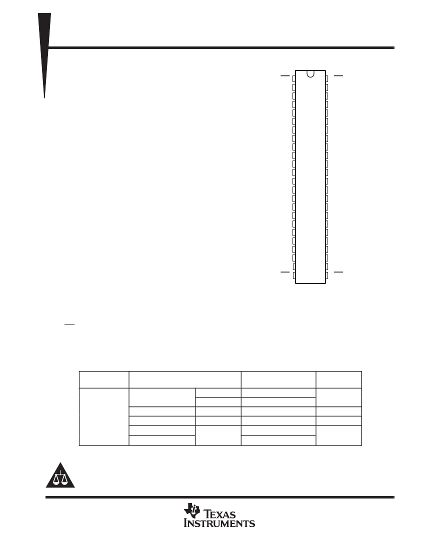
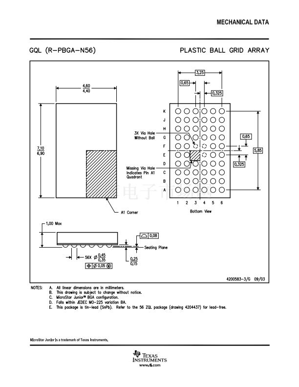
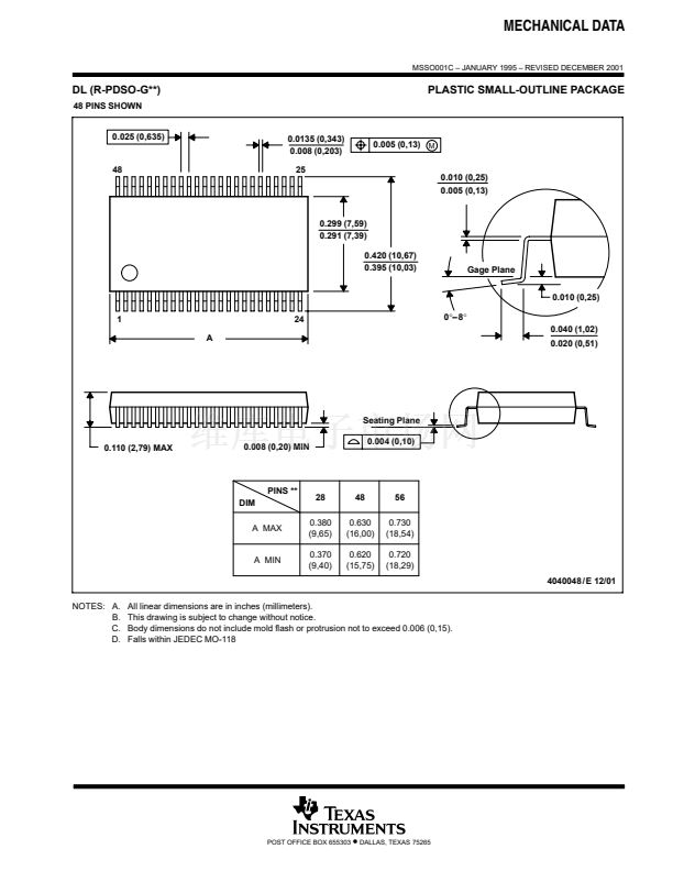
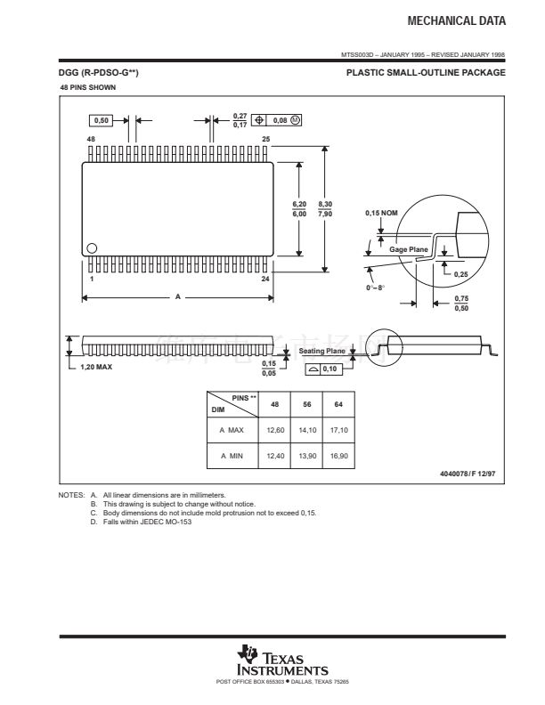
DGG, DGV, OR DL PACKAGE
(TOP VIEW)
description/ordering information
This 16-bit buffer/driver is designed for 1.65-V to
3.6-V V
CC
operation.
1OE
1Y1
1Y2
GND
1Y3
1Y4
V
CC
2Y1
2Y2
GND
2Y3
2Y4
3Y1
3Y2
GND
3Y3
3Y4
V
CC
4Y1
4Y2
GND
4Y3
4Y4
4OE
1
2
3
4
5
6
7
8
9
10
11
12
13
14
15
16
17
18
19
20
21
22
23
24
48
47
46
45
44
43
42
41
40
39
38
37
36
35
34
33
32
31
30
29
28
27
26
25
2OE
1A1
1A2
GND
1A3
1A4
V
CC
2A1
2A2
GND
2A3
2A4
3A1
3A2
GND
3A3
3A4
V
CC
4A1
4A2
GND
4A3
4A4
3OE
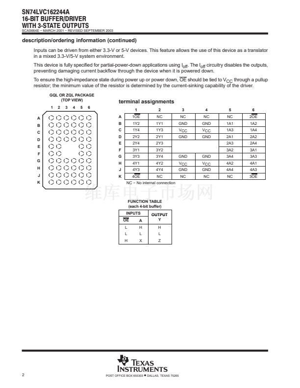
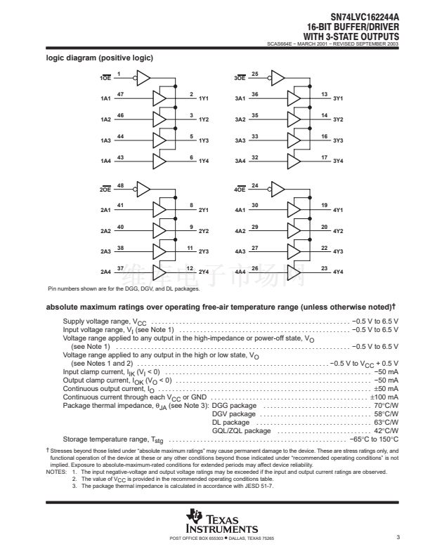
The SN74LVC162244A is designed specifically to improve both the performance and density of 3-state memory
address drivers, clock drivers, and bus-oriented receivers and transmitters. The device can be used as four 4-bit
buffers, two 8-bit buffers, or one 16-bit buffer. It provides true outputs and symmetrical active-low output-enable
(OE) inputs.
The outputs, which are designed to sink up to 12 mA, include equivalent 26-鈩?resistors to reduce overshoot
and undershoot.
ORDERING INFORMATION
TA
SSOP 鈭?DL
TSSOP 鈭?DGG
鈭?0擄C to 85擄C
TVSOP 鈭?DGV
VFBGA 鈭?GQL
VFBGA 鈭?ZQL (Pb-free)
Tape and reel
PACKAGE鈥?/div>
Tube
Tape and reel
Tape and reel
Tape and reel
ORDERABLE
PART NUMBER
SN74LVC162244ADL
SN74LVC162244ADLR
SN74LVC162244ADGGR
SN74LVC162244ADGVR
SN74LVC162244AGQLR
SN74LVC162244AZQLR
LD2244A
LVC162244A
LVC162244A
LD2244A
TOP-SIDE
MARKING
鈥?Package drawings, standard packing quantities, thermal data, symbolization, and PCB design guidelines are
available at www.ti.com/sc/package.
Please be aware that an important notice concerning availability, standard warranty, and use in critical applications of
Texas Instruments semiconductor products and disclaimers thereto appears at the end of this data sheet.
Widebus is a trademark of Texas Instruments.
PRODUCTION DATA information is current as of publication date.
Products conform to specifications per the terms of Texas Instruments
standard warranty. Production processing does not necessarily include
testing of all parameters.
Copyright
錚?/div>
2003, Texas Instruments Incorporated
POST OFFICE BOX 655303
鈥?/div>
DALLAS, TEXAS 75265
1


 1
1
 2
2
 3
3
 4
4
 5
5
 6
6
 7
7
 8
8
 9
9
 10
10
 11
11
 12
12
