SPICE MODEL: MMBTA63 MMBTA64
Pb
Lead-free
MMBTA63 / MMBTA64
PNP SURFACE MOUNT DARLINGTON TRANSISTOR
Features
路
路
路
路
路
Epitaxial Planar Die Construction
Complementary NPN Types Available
(MMBTA13 /MMBTA14)
Ideal for Low Power Amplification and Switching
High Current Gain
Lead Free/RoHS Compliant Version (Note 3)
B
TOP VIEW
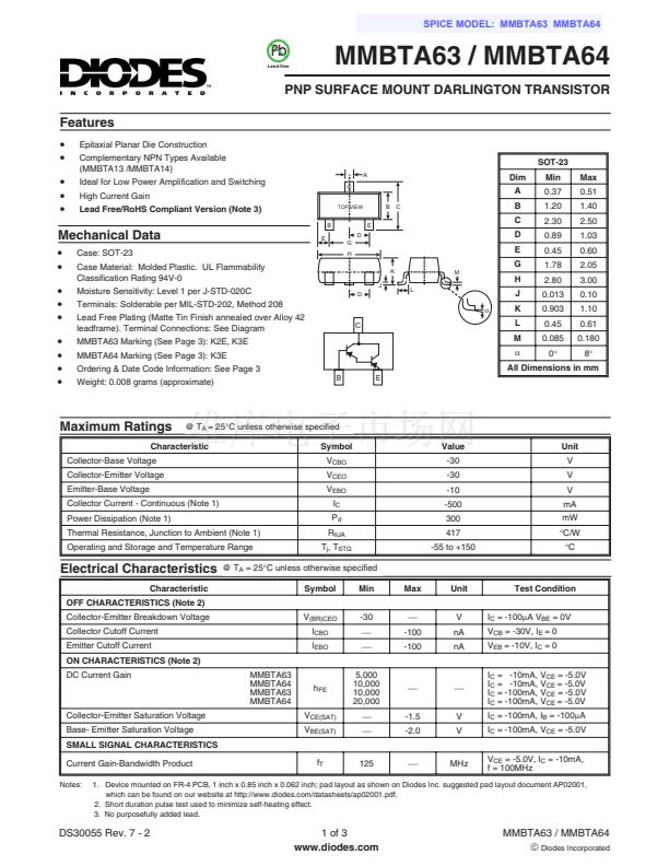
SOT-23
A
C
B
E
D
G
H
K
J
D
L
M
C
Dim
A
B
C
D
E
G
H
J
K
L
M
a
Min
0.37
1.20
2.30
0.89
0.45
1.78
2.80
0.013
0.903
0.45
0.085
0擄
Max
0.51
1.40
2.50
1.03
0.60
2.05
3.00
0.10
1.10
0.61
0.180
8擄
Mechanical Data
路
路
路
路
路
路
路
路
路
Case: SOT-23
Case Material: Molded Plastic. UL Flammability
Classification Rating 94V-0
Moisture Sensitivity: Level 1 per J-STD-020C
Terminals: Solderable per MIL-STD-202, Method 208
Lead Free Plating (Matte Tin Finish annealed over Alloy 42
leadframe). Terminal Connections: See Diagram
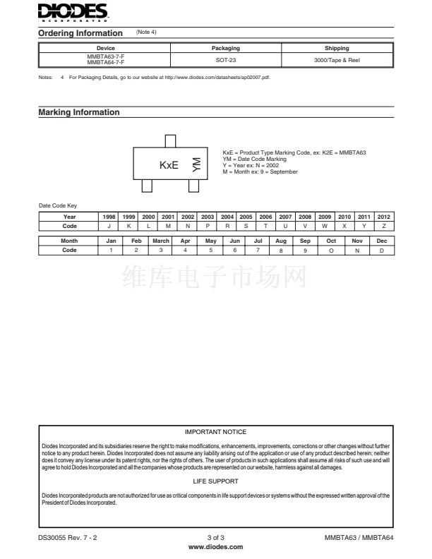
MMBTA63 Marking (See Page 3): K2E, K3E
MMBTA64 Marking (See Page 3): K3E
Ordering & Date Code Information: See Page 3
Weight: 0.008 grams (approximate)
E
C
All Dimensions in mm
B
E
Maximum Ratings
Collector-Base Voltage
Collector-Emitter Voltage
Emitter-Base Voltage
@ T
A
= 25擄C unless otherwise specified
Symbol
V
CBO
V
CEO
V
EBO
I
C
P
d
R
qJA
T
j
, T
STG
Value
-30
-30
-10
-500
300
417
-55 to +150
Unit
V
V
V
mA
mW
擄C/W
擄C
Characteristic
Collector Current - Continuous (Note 1)
Power Dissipation (Note 1)
Thermal Resistance, Junction to Ambient (Note 1)
Operating and Storage and Temperature Range
Electrical Characteristics
Characteristic
OFF CHARACTERISTICS (Note 2)
Collector-Emitter Breakdown Voltage
Collector Cutoff Current
Emitter Cutoff Current
ON CHARACTERISTICS (Note 2)
DC Current Gain
@ T
A
= 25擄C unless otherwise specified
Symbol
V
(BR)CEO
I
CBO
I
EBO
MMBTA63
MMBTA64
MMBTA63
MMBTA64
Min
-30
戮
戮
5,000
10,000
10,000
20,000
戮
戮
Max
戮
-100
-100
Unit
V
nA
nA
Test Condition
I
C
= -100mA V
BE
= 0V
V
CB
= -30V, I
E
= 0
V
EB
= -10V, I
C
= 0
I
C
= -10mA, V
CE
= -5.0V
I
C
= -10mA, V
CE
= -5.0V
I
C
= -100mA, V
CE
= -5.0V
I
C
= -100mA, V
CE
= -5.0V
I
C
= -100mA, I
B
= -100mA
I
C
= -100mA, V
CE
= -5.0V
V
CE
= -5.0V, I
C
= -10mA,
f = 100MHz
h
FE
V
CE(SAT)
V
BE(SAT)
戮
-1.5
-2.0
戮
V
V
Collector-Emitter Saturation Voltage
Base- Emitter Saturation Voltage
SMALL SIGNAL CHARACTERISTICS
Current Gain-Bandwidth Product
Notes:
f
T
125
戮
MHz
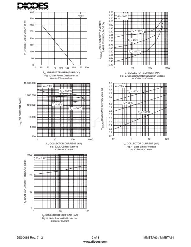
1. Device mounted on FR-4 PCB, 1 inch x 0.85 inch x 0.062 inch; pad layout as shown on Diodes Inc. suggested pad layout document AP02001,
which can be found on our website at http://www.diodes.com/datasheets/ap02001.pdf.
2. Short duration pulse test used to minimize self-heating effect.
3. No purposefully added lead.
DS30055 Rev. 7 - 2
1 of 3
www.diodes.com
MMBTA63 / MMBTA64
茫
Diodes Incorporated


 1
1
 2
2
 3
3
