鈥?/div>
Single 3.3 V
鹵
10% Power Supply
Fast Access Time: 10/11/12/15 ns
Equal Address and Chip Enable Access Time
All Inputs and Outputs are TTL Compatible
Three鈥揝tate Outputs
Power Operation: 280/275/270/260 mA Maximum, Active AC
Commercial Temperature (0擄C to 70擄C) and
Industrial Temperature (鈥?40擄C to + 85擄C) Options
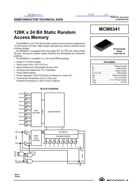
BLOCK DIAGRAM
A
A
A
A
A
A
A
A
A
ROW
DECODER
ZP PACKAGE
PBGA
CASE 999鈥?2
PIN NAMES
A . . . . . . . . . . . . . . . . . . . . . . Address Inputs
W . . . . . . . . . . . . . . . . . . . . . . . Write Enable
G . . . . . . . . . . . . . . . . . . . . . Output Enable
E1, E2, E3 . . . . . . . . . . . . . . . . Chip Enable
DQ . . . . . . . . . . . . . . . . . Data Input/Output
NC . . . . . . . . . . . . . . . . . . . . No Connection
VDD . . . . . . . . . . . . . + 3.3 V Power Supply
VSS . . . . . . . . . . . . . . . . . . . . . . . . . Ground
MEMORY MATRIX
DQ
INPUT
DATA
CONTROL
DQ
A
E1
E2
E3
W
G
A
A
COLUMN I/O
COLUMN DECODER
A
A
A
A
A
DQ
DQ
This document contains information on a new product. Specifications and information herein are subject to change without notice.
REV 2
2/18/98
漏
Motorola, Inc. 1998
MOTOROLA FAST SRAM
MCM6341
1


 1
1
 2
2
 3
3
 4
4
 5
5
 6
6
 7
7
 8
8
 9
9
 10
10
