MC10E451, MC100E451
5V ECL 6鈭払it D Register
Differential Data and Clock
Description
The MC10E/100E451 contains six D鈭抰ype flip鈭抐lops with
single鈭抏nded outputs and differential data inputs. The common clock
input is also differential. The registers are triggered by a positive
transition of the positive clock (CLK) input.
A HIGH on the Master Reset (MR) input resets all Q outputs to
LOW.
The differential input structures are clamped so that the inputs of
unused registers can be left open without upsetting the bias network of
the device. The clamping action will assert the D and the CLK sides of
the inputs. Because of the edge triggered flip鈭抐lop nature of the device
simultaneously opening both the clock and data inputs will result in an
output which reaches an unidentified but valid state. Note that the
input clamps only operate when both inputs fall to 2.5 V below V
CC
.
The V
BB
pin, an internally generated voltage supply, is available to
this device only. For single鈭抏nded input conditions, the unused
differential input is connected to V
BB
as a switching reference voltage.
V
BB
may also rebias AC coupled inputs. When used, decouple V
BB
and V
CC
via a 0.01
mF
capacitor and limit current sourcing or sinking
to 0.5 mA. When not used, V
BB
should be left open.
The 100 Series contains temperature compensation.
Features
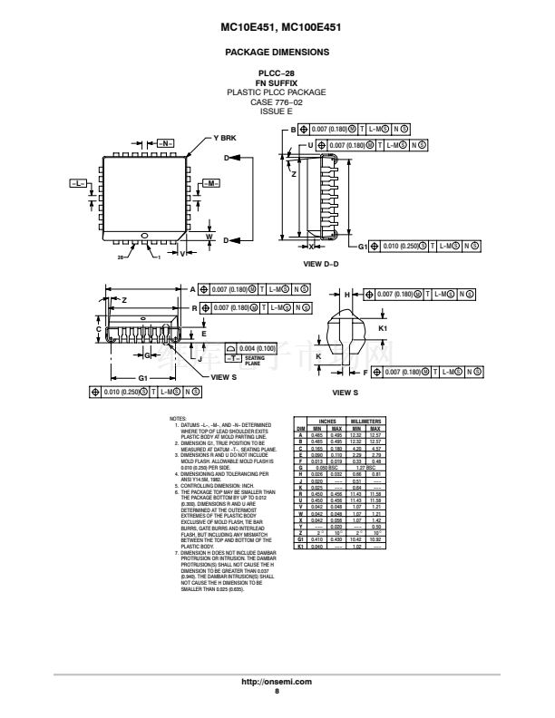
http://onsemi.com
PLCC鈭?8
FN SUFFIX
CASE 776
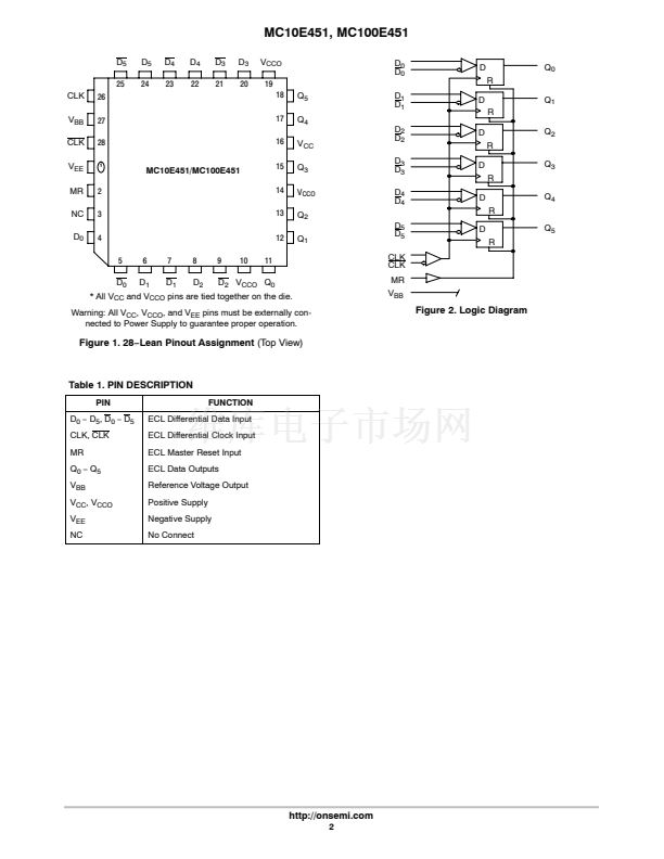
MARKING DIAGRAM*
1 28
MCxxxE451FNG
AWLYYWW
鈥?/div>
鈥?/div>
鈥?/div>
鈥?/div>
鈥?/div>
鈥?/div>
鈥?/div>
鈥?/div>
鈥?/div>
鈥?/div>
鈥?/div>
Differential Inputs: Data and Clock
V
BB
Output
1100 MHz Min. Toggle Frequency
Asynchronous Master Reset
PECL Mode Operating Range:
V
CC
= 4.2 V to 5.7 V with V
EE
= 0 V
NECL Mode Operating Range:
V
CC
= 0 V with V
EE
=
鈭?.2
V to
鈭?.7
V
Internal Input 50 kW Pulldown Resistors
ESD Protection: Human Body Model; > 2 kV,
Machine Model; > 200 V
Transistor Count = 348 devices
Meets or Exceeds JEDEC Spec EIA/JESD78 IC
Latchup Test
Flammability Rating: UL 94 V鈭? @ 0.125 in,
Oxygen Index: 28 to 34
xxx
A
WL
YY
WW
G
= 10 or 100
= Assembly Location
= Wafer Lot
= Year
= Work Week
= Pb鈭扚ree Package
*For additional marking information, refer to
Application Note AND8002/D.
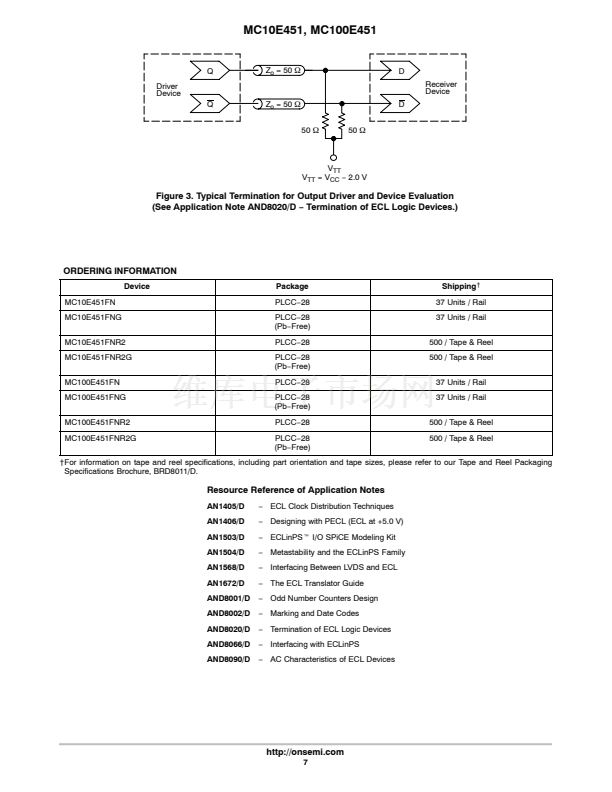
ORDERING INFORMATION
See detailed ordering and shipping information in the package
dimensions section on page 7 of this data sheet.
鈥?/div>
Moisture Sensitivity Level:
Pb = 1;
Pb鈭扚ree = 3
For Additional Information, see Application Note
AND8003/D
鈥?/div>
Pb鈭扚ree Packages are Available*
*For additional information on our Pb鈭扚ree strategy and soldering details, please
download the ON Semiconductor Soldering and Mounting Techniques
Reference Manual, SOLDERRM/D.
漏
Semiconductor Components Industries, LLC, 2006
November, 2006
鈭?/div>
Rev. 9
1
Publication Order Number:
MC10E451/D
MC100E451FNG PDF文件相關(guān)型號(hào)
MC100E451FNR2,MC100E451FNR2G,MC10E451FNG,MC10E451FNR2
MC100E451FNG 產(chǎn)品屬性
37
集成電路 (IC)
邏輯 - 觸發(fā)器
100E
主復(fù)位
D 型總線
非反相
1
6
1.1GHz
625ps
正邊沿
-
4.2 V ~ 5.7 V
0°C ~ 85°C
表面貼裝
28-LCC(J 形引線)
管件
MC100E451FNG相關(guān)型號(hào)PDF文件下載


 1
1
 2
2
 3
3
 4
4
 5
5
 6
6
 7
7
 8
8
 9
9
