MC10E416, MC100E416
5V ECL Quint Differential
Line Receiver
Description
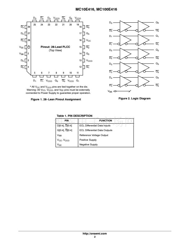
The MC10E416/100E416 is a 5-bit differential line receiving device.
The 2.0 GHz of bandwidth provided by the high frequency outputs
makes the device ideal for buffering of very high speed oscillators.
The design incorporates two stages of gain, internal to the device,
making it an excellent choice for use in high bandwidth amplifier
applications.
The differential inputs have internal clamp structures which will
force the Q output of a gate in an open input condition to go to a LOW
state. Thus, inputs of unused gates can be left open and will not affect
the operation of the rest of the device. Note that the input clamp will
take affect only if both inputs fall 2.5 V below V
CC
.
The V
BB
pin, an internally generated voltage supply, is available to
this device only. For single-ended input conditions, the unused
differential input is connected to V
BB
as a switching reference voltage.
V
BB
may also rebias AC coupled inputs. When used, decouple V
BB
and V
CC
via a 0.01
mF
capacitor and limit current sourcing or sinking
to 0.5 mA. When not used, V
BB
should be left open.
The 100 Series contains temperature compensation.
Features
http://onsemi.com
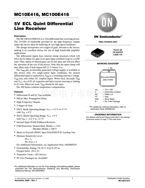
PLCC鈭?8
FN SUFFIX
CASE 776
MARKING DIAGRAM*
1 28
MCxxxE416FNG
AWLYYWW
鈥?/div>
鈥?/div>
鈥?/div>
鈥?/div>
鈥?/div>
Differential D and Q; V
BB
available
600 ps Max. Propagation Delay
High Frequency Outputs
2 Stages of Gain
xxx
A
WL
YY
WW
G
= 10 or 100
= Assembly Location
= Wafer Lot
= Year
= Work Week
= Pb鈭扚ree Package
PECL Mode Operating Range: V
CC
= 4.2 V to 5.7 V
with V
EE
= 0 V
鈥?/div>
NECL Mode Operating Range: V
CC
= 0 V
with V
EE
=
鈭?.2
V to
鈭?.7
V
鈥?/div>
Internal Input 50 kW Pulldown Resistors
*For additional marking information, refer to
Application Note AND8002/D.
ORDERING INFORMATION
See detailed ordering and shipping information in the package
dimensions section on page 7 of this data sheet.
鈥?/div>
ESD Protection: Human Body Model; > 2 kV,
鈥?/div>
Moisture Sensitivity Level:
Machine Model; > 200 V
鈥?/div>
Meets or Exceeds JEDEC Spec EIA/JESD78 IC Latchup Test
Pb = 1;
Pb鈭扚ree = 3
For Additional Information, see Application Note AND8003/D
鈥?/div>
Flammability Rating: UL 94 V鈭? @ 0.125 in,
Oxygen Index: 28 to 34
鈥?/div>
Transistor Count = 201 devices
鈥?/div>
Pb鈭扚ree Packages are Available*
*For additional information on our Pb鈭扚ree strategy and soldering details, please
download the ON Semiconductor Soldering and Mounting Techniques
Reference Manual, SOLDERRM/D.
漏
Semiconductor Components Industries, LLC, 2006
November, 2006
鈭?/div>
Rev. 7
1
Publication Order Number:
MC10E416/D
MC100E416FNG PDF文件相關(guān)型號
MC100E416FNR2,MC100E416FNR2G,MC10E416FNG,MC10E416FNR2,MC10E416FNR2G
MC100E416FNG 產(chǎn)品屬性
37
集成電路 (IC)
邏輯 - 專用邏輯
100E
差分接收器
4.2 V ~ 5.7 V
5
0°C ~ 85°C
表面貼裝
28-LCC(J 形引線)
28-PLCC(11.51x11.51)
管件
MC100E416FNG相關(guān)型號PDF文件下載


 1
1
 2
2
 3
3
 4
4
 5
5
 6
6
 7
7
 8
8
 9
9
