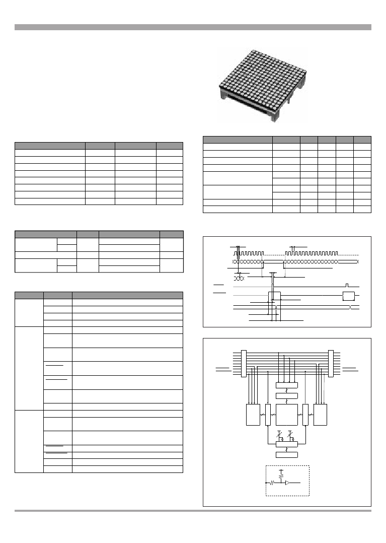
Dot Matrix LED Unit for Indoor Use LT1451ED(Chip On Board Type)
s
Features
隆No.
of dots : 16!16dots
隆Outline
dimensions : 96!96mm
隆Dot
size : 酶5.0mm
隆Dot
pitch : 6.0mm
隆Radiation
color : Yellow-green+Red(dichromatic type)
隆Driving
method : 1/16 duty dynamic drive
LT1451ED
s
Absolute Maximum Ratings
Parameter
Supply voltage for IC
Supply voltage for LED
Input voltage
LED current dissipation
Turn-on time
Operating temperature
Storage temperature
Power dissipation
Symbol
V
CC
V
LED
V
I
I
LED
t
ON
T
opr
T
stg
P
Rating
-0.3 to +6.0
-0.3 to +6.0
-0.3 to Vcc+0.3
1
-10 to +45
-20 to +70
13
s
Electrical Characteristics
(Ta=25藲C)
(V
CC
=5V,V
LED
=5V,Ta=25藲C)
Unit
V
V
V
A
ms
藲C
藲C
W
Symbol MIN. TYP. MAX. Unit
V
5.25
5.0
V
CC
4.75
V
5.25
5.0
4.5
V
LED
------
mA
50
25
I
CC
------
A
2.3
2.0
I
LED
------
------
V
3.5
V
IH
Input voltage
------
------
V
1.5
V
IL
------
------
碌A(chǔ)
0.1
I
IH
Input current
------
------
0.12
I
IL
mA
------
------
4
f
CLK
MH
Z
Clock frequency
------
625
80
Frame frequency
f
FR
H
Z
*1 Under the condition that dichromatic all dots are lit.
Parameter
Supply voltage for IC
Supply voltage for LED
IC current dissipation
*1
LED current dissipation
*1
s
Optical Characteristics
Parameter
Red
Yellow-green
Viewing angle
Red
Peak emission wavelength
Yellow-green
Luminance
Symbol
L
V
2胃
1
/
2
位p
(V
CC
=5V,V
LED
=5V,Ta=25藲C)
TYP.
100
100
70
635
565
Unit
cd/m
藲
nm
2
s
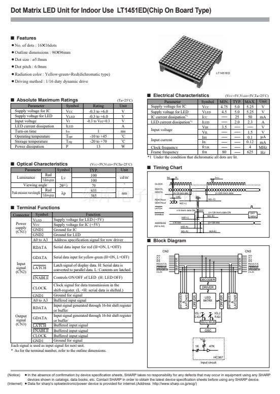
Timing Chart
tsu
CLOCK
RDATA,
GDATA
RDATAout
GDATAout
th
t
WCLK
(n+1)th line's data
t dD
td(C-L)
n th line's data ON
OFF
tWL
(n+2)th line's data
td(L-C)
s
Terminal Functions
Connector
Power
supply
(CN1)
Symbol
V
LED
V
CC
GND1
GND2
A0 to A3
RDATA
GDATA
Input
signal
(CN2)
LATCH
ENABLE
CLOCK
Function
Supply voltage for LED (+5V)
Supply voltage for IC (+5V)
Ground for IC
Ground for LED
Address specification signal for row driver
Serial data input for red (H=ON, L=OFF)
LATCH
ENABLE
td(E-L)
ADDRESS
(A0 to A3)
n th line
td(E-A)
td(L-A)
td(A-E)
(n+1)th line's data ON
td(L-E)
(n+1)th line
OFF
t WENA
s
Block Diagram
CN2
BUFFER
BUFFER
DECODER
DRIVER
SHIFT REGISTER
&
LATCH(G)
LED
MATRIX
SHIFT REGISTER
&
LATCH(R)
DRIVER
DRIVER
VOL.1
G.ADJ
VOL.2
R.ADJ
Mono-Multi
OSC
Vcc
CN3
A0
A1
A2
A3
RDATA
GDATA
LATCH
ENABLE
CLK
Serial data input for yellow-green (H=ON, L=OFF)
Latch signal of display data. H: Serial data is
converted to parallel data. L: Contents are latched.
Controls ON/OFF of LED (H: LED OFF)
A0
A1
A2
A3
RDATA
GDATA
LATCH
ENABLE
CLK
Clock signal for data transmission in the
shift-register. (L隆H: serial data is shifted.)
Ground for signal
GND1
A0 to A3 Buffered input signal
Input signal generated through 16-bit shift register
RDATA
or buffer
Input signal generated through 16-bit shift register
Output
GDATA
signal
or buffer
(CN3)
Buffered input signal
LATCH
ENABLE Buffered input signal
CLOCK
Buffered input signal
Ground for signal
GND1
Each signal is used as input signal for next unit.
* As for the terminal number, refer to the outline dimensions.
1K
47K
HC367
Input circuit
隆In
the absence of confirmation by device specification sheets, SHARP takes no responsibility for any defects that may occur in equipment using any SHARP
devices shown in catalogs, data books, etc. Contact SHARP in order to obtain the latest device specification sheets before using any SHARP device.
(Internet)
隆Data
for sharp's optoelectronic/power device is provided for internet.(Address http://www.sharp.co.jp/ecg/)
(Notice)
16


 1
1
 2
2
