IDT74LVCH245A
3.3V CMOS OCTAL BUS TRANSCEIVER WITH 3-STATE OUTPUTS
INDUSTRIAL TEMPERATURE RANGE
3.3V CMOS OCTAL BUS
TRANSCEIVER WITH 3-STATE
OUTPUTS, 5 VOLT TOLERANT I/O
AND BUS-HOLD
鈥?0.5 MICRON CMOS Technology
鈥?ESD > 2000V per MIL-STD-883, Method 3015; > 200V using
machine model (C = 200pF, R = 0)
鈥?V
CC
= 3.3V 鹵 0.3V, Normal Range
鈥?V
CC
= 2.7V to 3.6V, Extended Range
鈥?CMOS power levels (0.4碌 W typ. static)
碌
鈥?Rail-to-rail output swing for increased noise margin
鈥?All inputs, outputs, and I/O are 5V tolerant
鈥?Supports hot insertion
鈥?Available in SOIC, SSOP, QSOP, and TSSOP packages
IDT74LVCH245A
FEATURES:
DESCRIPTION:
DRIVE FEATURES:
APPLICATIONS:
鈥?High Output Drivers: 鹵24mA
鈥?Reduced system switching noise
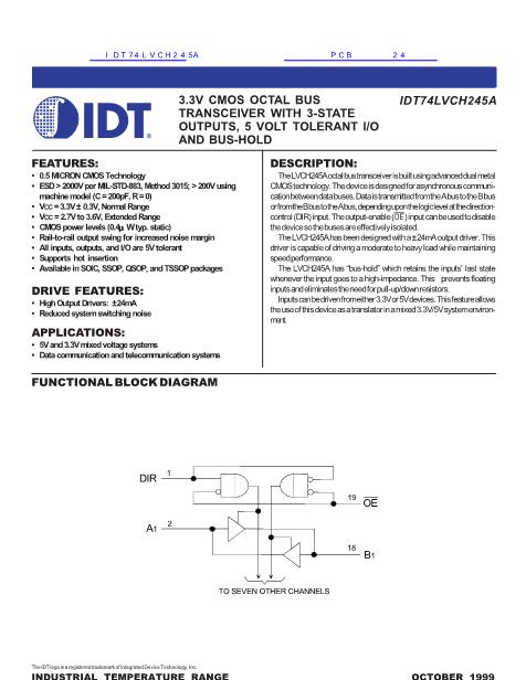
The LVCH245A octal bus transceiver is built using advanced dual metal
CMOS technology. The device is designed for asynchronous communi-
cation between data buses. Data is transmitted from the A bus to the B bus
or from the B bus to the A bus, depending upon the logic level at the direction-
control (DIR) input. The output-enable (OE) input can be used to disable
the device so the buses are effectively isolated.
The LVCH245A has been designed with a 鹵24mA output driver. This
driver is capable of driving a moderate to heavy load while maintaining
speed performance.
The LVCH245A has 鈥渂us-hold鈥?which retains the inputs鈥?last state
whenever the input goes to a high-impedance. This prevents floating
inputs and eliminates the need for pull-up/down resistors.
Inputs can be driven from either 3.3V or 5V devices. This feature allows
the use of this device as a translator in a mixed 3.3V/5V system environ-
ment.
鈥?5V and 3.3V mixed voltage systems
鈥?Data communication and telecommunication systems
FUNCTIONAL BLOCK DIAGRAM
DIR
1
19
2
18
OE
A
1
B
1
TO SEVEN OTHER CHANNELS
The IDT logo is a registered trademark of Integrated Device Technology, Inc.
INDUSTRIAL TEMPERATURE RANGE
1
漏 1999 Integrated Device Technology, Inc.
OCTOBER 1999
DSC-4611/1


 1
1
 2
2
 3
3
 4
4
 5
5
 6
6
