IDT74LVCH162245A
3.3V CMOS 16-BIT BUS TRANSCEIVER WITH 5V TOLERANT I/O
INDUSTRIAL TEMPERATURE RANGE
3.3V CMOS 16-BIT
BUS TRANSCEIVER
WITH 5 VOLT TOLERANT I/O
AND BUS-HOLD
鈥?Typical t
SK(o)
(Output Skew) < 250ps
鈥?ESD > 2000V per MIL-STD-883, Method 3015; > 200V using
machine model (C = 200pF, R = 0)
鈥?V
CC
= 3.3V 鹵 0.3V, Normal Range
鈥?V
CC
= 2.7V to 3.6V, Extended Range
鈥?CMOS power levels (0.4碌 W typ. static)
碌
鈥?All inputs, outputs, and I/O are 5V tolerant
鈥?Available in SSOP, TSSOP, and TVSOP packages
IDT74LVCH162245A
FEATURES:
DESCRIPTION:
DRIVE FEATURES:
APPLICATIONS:
鈥?Balanced Output Drivers: 鹵12mA (A port)
鈥?High Output Drivers: 鹵24mA (B port)
鈥?5V and 3.3V mixed voltage systems
鈥?Data communication and telecommunication systems
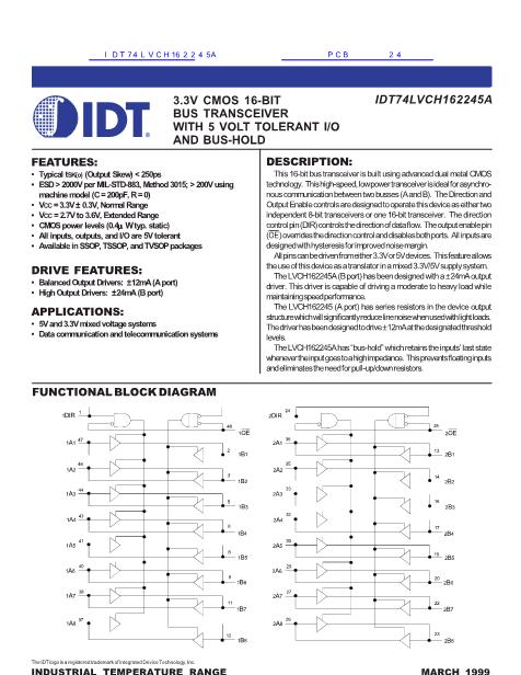
This 16-bit bus transceiver is built using advanced dual metal CMOS
technology. This high-speed, low power transceiver is ideal for asynchro-
nous communication between two busses (A and B). The Direction and
Output Enable controls are designed to operate this device as either two
independent 8-bit transceivers or one 16-bit transceiver. The direction
control pin (DIR) controls the direction of data flow. The output enable pin
(OE) overrides the direction control and disables both ports. All inputs are
designed with hysteresis for improved noise margin.
All pins can be driven from either 3.3V or 5V devices. This feature allows
the use of this device as a translator in a mixed 3.3V/5V supply system.
The LVCH162245A (B port) has been designed with a 鹵24mA output
driver. This driver is capable of driving a moderate to heavy load while
maintaining speed performance.
The LVCH162245 (A port) has series resistors in the device output
structure which will significantly reduce line noise when used with light loads.
The driver has been designed to drive 鹵12mA at the designated threshold
levels.
The LVCH162245A has 鈥渂us-hold鈥?which retains the inputs鈥?last state
whenever the input goes to a high impedance. This prevents floating inputs
and eliminates the need for pull-up/down resistors.
FUNCTIONAL BLOCK DIAGRAM
1
DIR
1
48
24
2
DIR
25
1
OE
1
A
1
47
2
46
2
OE
2
A
1
36
13
35
1
B
1
2
A
2
2
B
1
1
A
2
3
1
B
2
1
A
3
44
5
43
6
33
14
2
B
2
2
A
3
16
1
B
3
32
2
B
3
2
A
4
17
1
A
4
1
B
4
1
A
5
41
8
2
B
4
2
A
5
30
19
1
B
5
1
A
6
40
9
2
B
5
2
A
6
1
B
6
29
20
27
22
2
B
6
1
A
7
38
11
2
A
7
1
B
7
2
B
7
2
A
8
26
23
1
A
8
37
12
1
B
8
2
B
8
The IDT logo is a registered trademark of Integrated Device Technology, Inc.
INDUSTRIAL TEMPERATURE RANGE
1
漏 1999 Integrated Device Technology, Inc.
MARCH 1999
DSC-4597/1


 1
1
 2
2
 3
3
 4
4
 5
5
 6
6
 7
7
