HCC/HCF4093B
QUAD 2-INPUT NAND SCHMIDT TRIGGERS
.
.
.
.
.
.
.
.
.
.
SCHMITT-TRIGGER ACTION ON EACH INPUT
WITH NO EXTERNAL COMPONENTS
HYSTERESIS VOLTAGE TYPICALLY 0.9V AT
V
DD
= 5V AND 2.3V AT V
DD
= 10V
NOISE IMMUNITY GREATER THAN 50% OF
V
DD
(typ.)
NO LIMIT ON INPUT RISE AND FALL TIMES
STANDARDIZED SYMMETRICAL OUTPUT
CHARACTERISTICS
QUIESCENT CURRENT SPECIFIED TO 20V
FOR HCC DEVICE
5V, 10V, AND 15V PARAMETRIC RATINGS
INPUT CURRENT OF 100nA AT 18V AND
25擄C FOR HCC DEVICE
100% TESTED FOR QUIESCENT CURRENT
MEETS ALL REQUIREMENTS OF JEDEC TEN-
TATIVE STANDARD N擄. 13A, 鈥漇TANDARD
SPECIFICATIONS FOR DESCRIPTION OF 鈥滲鈥?/div>
SERIES CMOS DEVICES鈥?/div>
EY
(Plastic Package)
F
(Ceramic Frit Seal Package)
M1
(Micro Package)
C1
(Plastic Chip Carrier)
ORDER CODES :
HCC4093BF
HCF4093BM1
HCF4093BEY
HCF4093BC1
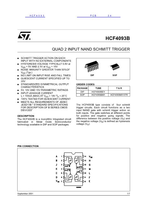
PIN CONNECTIONS
DESCRIPTION
The
HCC4093B
(extended temperature range) and
HCF4093B
(intermediate temperature range) are
available in 14-lead dual in-line plastic or ceramic
package and plastic micropackage. The
HCC/HCF4093B
consists of four Schmitt-trigger cir-
cuits. Each circuit functions as a two-input NAND
gate with Schmitt-trigger action on both inputs. The
gate switches at different points for positive and ne-
gative-going signals.
The difference between the positive voltage (V
P
)
and the negative voltage (V
N
) is defined as hys-
teresis voltage (V
H
) (see fig. 1).
June 1989
1/13


 1
1
 2
2
 3
3
 4
4
 5
5
 6
6
 7
7
 8
8
 9
9
 10
10
 11
11
 12
12
 13
13
