鈥?/div>
Extra data width for wide address/data paths or buses carrying
parity
DESCRIPTION
The 74ABT841 Bus interface register is designed to provide extra
data width for wider data/address paths of buses carrying parity.
The 74ABT841 consists of ten D-type latches with 3-State outputs.
The flip-flops appear transparent to the data when Latch Enable
(LE) is High. This allows asynchronous operation, as the output
transition follows the data in transition. On the LE High-to-Low
transition, the data that meets the setup and hold time is latched.
Data appears on the bus when the Output Enable (OE) is Low.
When OE is High the output is in the High-impedance state.
鈥?/div>
Ideal where high speed, light loading, or increased fan-in are
required with MOS microprocessors
鈥?/div>
Slim DIP 300 mil package
鈥?/div>
Broadside pinout
鈥?/div>
Output capability: +64mA/鈥?2mA
鈥?/div>
Latch-up protection exceeds 500mA per Jedec Std 17
鈥?/div>
ESD protection exceeds 2000 V per MIL STD 883 Method 3015
and 200 V per Machine Model
鈥?/div>
Power-up 3-State
鈥?/div>
Power-up reset
QUICK REFERENCE DATA
SYMBOL
t
PLH
t
PHL
C
IN
C
OUT
I
CCZ
PARAMETER
Propagation delay
Dn to Qn
Input capacitance
Output capacitance
Total supply current
CONDITIONS
T
amb
= 25擄C; GND = 0V
C
L
= 50pF; V
CC
= 5V
V
I
= 0V or V
CC
Outputs disabled;
V
O
= 0V or V
CC
Outputs disabled; V
CC
= 5.5V
TYPICAL
4.1
4
7
500
UNIT
ns
pF
pF
nA
ORDERING INFORMATION
PACKAGES
24-Pin Plastic DIP
24-Pin plastic SO
24-Pin Plastic SSOP Type II
24-Pin Plastic TSSOP Type I
TEMPERATURE RANGE
鈥?0擄C to +85擄C
鈥?0擄C to +85擄C
鈥?0擄C to +85擄C
鈥?0擄C to +85擄C
OUTSIDE NORTH AMERICA
74ABT841 N
74ABT841 D
74ABT841 DB
74ABT841 PW
NORTH AMERICA
74ABT841 N
74ABT841 D
74ABT841 DB
74ABT841PW DH
DWG NUMBER
SOT222-1
SOT137-1
SOT340-1
SOT355-1
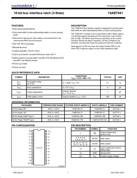
PIN CONFIGURATION
OE
D0
D1
D2
D3
D4
D5
D6
D7
1
2
3
4
5
6
7
8
9
TOP VIEW
24
23
22
21
20
19
18
17
16
15
14
13
V
CC
Q0
Q1
Q2
Q3
Q4
Q5
Q6
Q7
Q8
Q9
LE
PIN DESCRIPTION
PIN NUMBER
1
2, 3, 4, 5, 6,
7, 8, 9, 10, 11
23, 22, 21, 20, 19,
18, 17, 16, 15, 14
13
12
24
SYMBOL
OE
D0-D9
Q0-Q9
LE
GND
V
CC
FUNCTION
Output enable input
(active-Low)
Data inputs
Data outputs
Latch enable input (active
falling edge)
Ground (0V)
Positive supply voltage
D8 10
D9 11
GND 12
SA00247
1995 Sep 06
1
853-1628 15703
74ABT841相關(guān)型號PDF文件下載


 1
1
 2
2
 3
3
 4
4
 5
5
 6
6
