Silicon Junction FETs (Small Signal)
2SK1842
Silicon N-Channel Junction FET
For impedance conversion in low frequency
For infrared sensor
0.65鹵0.15
+0.2
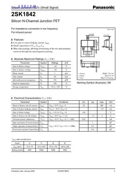
unit: mm
0.65鹵0.15
2.8
鈥?.3
1.5
鈥?.05
+0.25
s
Features
q
Low gate to source leakage current, I
GSS
q
Small capacitance of C
iss
, C
oss
, C
rss
q
Mini-type package, allowing downsizing of the sets and automatic
insertion through the tape/magazine packing.
0.95
2.9
鈥?.05
1
1.9鹵0.2
+0.2
0.95
3
0.4
鈥?.05
+0.1
2
Gate to Drain voltage
Gate to Source voltage
Drain current
Gate current
Allowable power dissipation
Junction temperature
Storage temperature
V
GSO
I
D
I
G
P
D
T
j
T
stg
鈭?0
1
10
150
150
鈭?5
to +150
V
mA
mA
mW
擄C
擄C
1: Source
2: Drain
3: Gate
JEDEC: TO-236
EIAJ: SC-59
Mini Type Package (3-pin)
Marking Symbol (Example): EB
s
Electrical Characteristics
(Ta = 25擄C)
Parameter
Drain to Source cut-off current
Gate to Source leakage current
Gate to Drain voltage
Gate to Source cut-off voltage
Forward transfer admittance
Symbol
I
DSS*
I
GSS
V
GDS
V
GSC
| Y
fs
|
C
oss
Conditions
V
DS
= 10V, V
GS
= 0
V
GS
=
鈭?0V,
V
DS
= 0
I
G
=
鈭?0碌A(chǔ),
V
DS
= 0
V
DS
= 10V, I
D
= 1碌A(chǔ)
V
DS
= 10V, V
GS
= 0, f = 1kHz
V
DS
= 10V, V
GS
= 0, f = 1MHz
0.05
1
0.4
0.4
鈭?0
鈭?.3
鈭?
min
30
typ
max
200
鈭?/div>
0.5
Unit
碌A(chǔ)
nA
V
V
mS
pF
pF
pF
Input capacitance (Common Source) C
iss
Output capacitance (Common Source)
Reverse transfer capacitance (Common Source) C
rss
*
I
DSS
rank classification
Runk
I
DSS
(mA)
O
30 to 75
EBP
P
50 to 100
EBQ
Q
70 to 130
EBR
R
100 to 200
EBS
Marking Symbol
0 to 0.1
V
GDO
鈭?0
V
0.1 to 0.3
0.4鹵0.2
0.8
Parameter
Symbol
Ratings
Unit
1.1
鈥?.1
0.16
鈥?.06
+0.2
+0.1
s
Absolute Maximum Ratings
(Ta = 25擄C)
1.45
1


 1
1
 2
2
