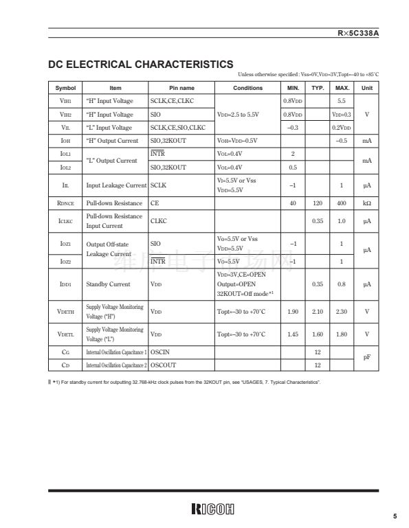
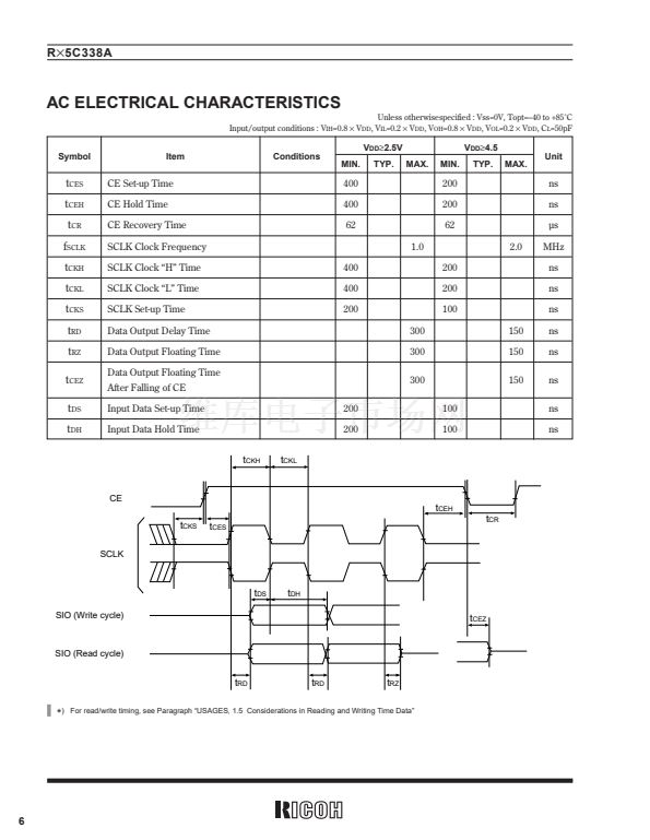
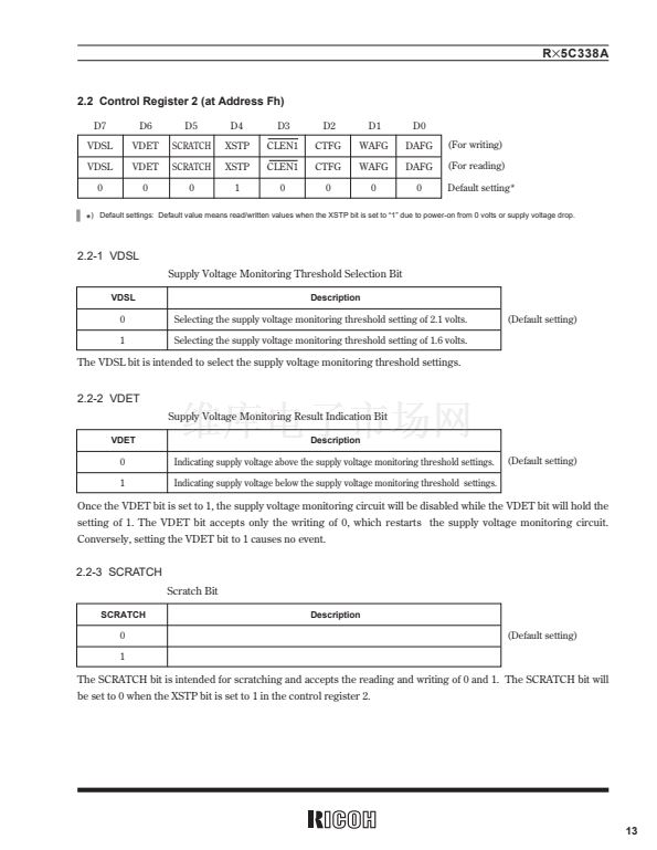
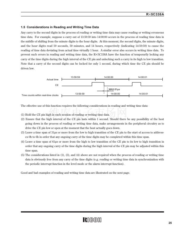
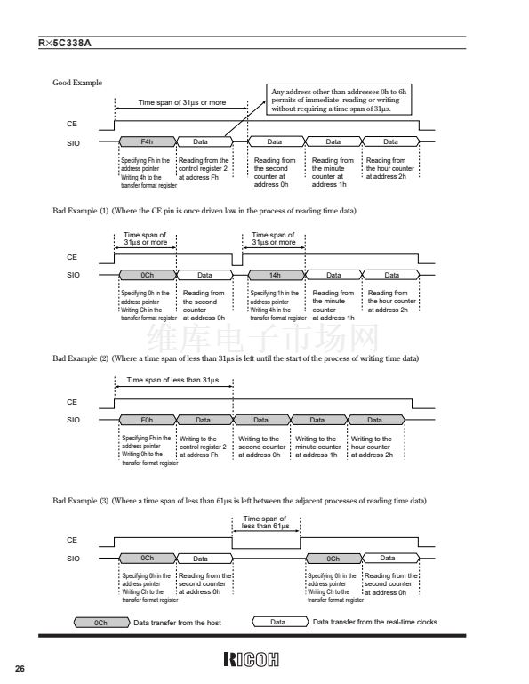
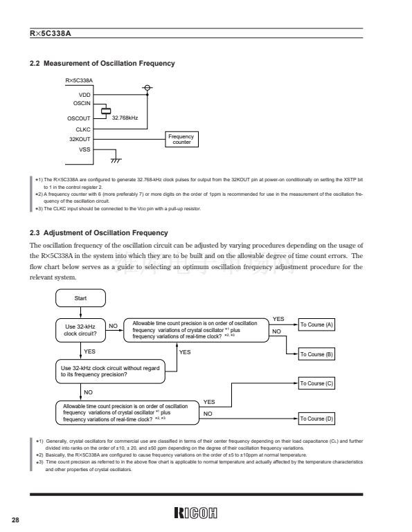
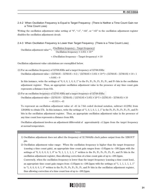
R
脳
5C338A
4. Alarm and Periodic Interrupt
The R
脳
5C338A incorporate the alarm circuit and the periodic interrupt circuit that are configured to generate alarm
signals and periodic interrupt signals, respectively, for output from the INTR pin as described below.
1)Alarm Circuit
The alarm interrupt circuit is configured to generate alarm signals for output from the INTR, which is driven low
(enabled) upon the occurrence of a match between current time read by the time counters (the day-of-week, hour,
and minute counters) and alarm time preset by the alarm registers (the Alarm_W registers intended for the day-
of-week, hour, and minute digit settings and the Alarm_D registers intended for the hour and minute digit set-
tings).
2)Periodic Interrupt Circuit
The periodic interrupt circuit is configured to generate either clock pulses in the pulse mode or interrupt signals
in the level mode for output from the INTR pin depending on the CT
2
, CT
1
, and CT
0
bit settings in the control reg-
ister 1.
The above two types of interrupt signals are monitored by the flag bits (i.e. the WAFG, DAFG, and CTFG bits in the
control register 2) and enabled or disabled by the enable bits (i.e. the WALE, DALE, CT
2
, CT
1
, and CT
0
bits in the
control register 1) as listed in the table below.
Flag bits
Enable bits
Alarm signals
(under control of Alarm_W registers)
Alarm signals
(under control of Alarm_D registers)
Periodic interrupt signals
WAFG bit
(D1 at Address Fh)
DAFG bit
(D0 at Address Fh)
CTFG bit
(D2 at Address Fh)
WALE bit
(D7 at Address Eh)
DALE bit
(D6 at Address Eh)
CT
2
, CT
1
, and CT
0
bits (D2 to D0 at Address Eh)
(these bit settings of 0 disable the periodic interrupt circuit)
路 At power-on, when the WALE, DALE, CT
2
, CT
1
, and CT
0
bits are set to 0 in the control register 1, the INTR pin is
driven high (disabled).
路 When two or more types of interrupt signals are output simultaneously from the INTR pin, the output from the
INTR pin becomes an OR waveform of their negative logic.
Example: Combined Output of Alarm Interrupt Signals from the INTR pin Under Control of Alarm_D and
Alarm_W Registers
Alarm_W
Alarm_D
INTR
In this event, which type of interrupt signal is output from the INTR pin can be confirmed by reading the
WAFG, DAFG, and CTFG bit settings in the control register 2.
34


 1
1
 2
2
 3
3
 4
4
 5
5
 6
6
 7
7
 8
8
 9
9
 10
10
 11
11
 12
12
 13
13
 14
14
 15
15
 16
16
 17
17
 18
18
 19
19
 20
20
 21
21
 22
22
 23
23
 24
24
 25
25
 26
26
 27
27
 28
28
 29
29
 30
30
 31
31
 32
32
 33
33
 34
34
 35
35
 36
36
 37
37
 38
38
 39
39
 40
40
 41
41
 42
42
 43
43
 44
44
 45
45
 46
46
 47
47
 48
48
 49
49
 50
50
 51
51
 52
52
