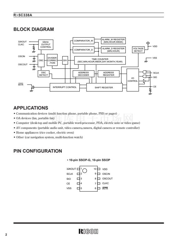
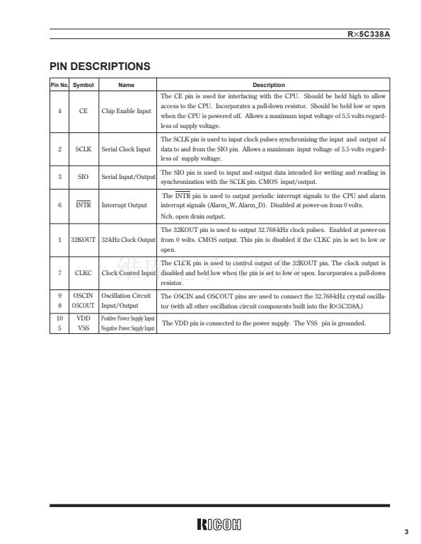
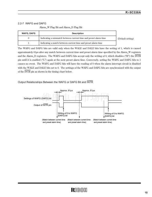
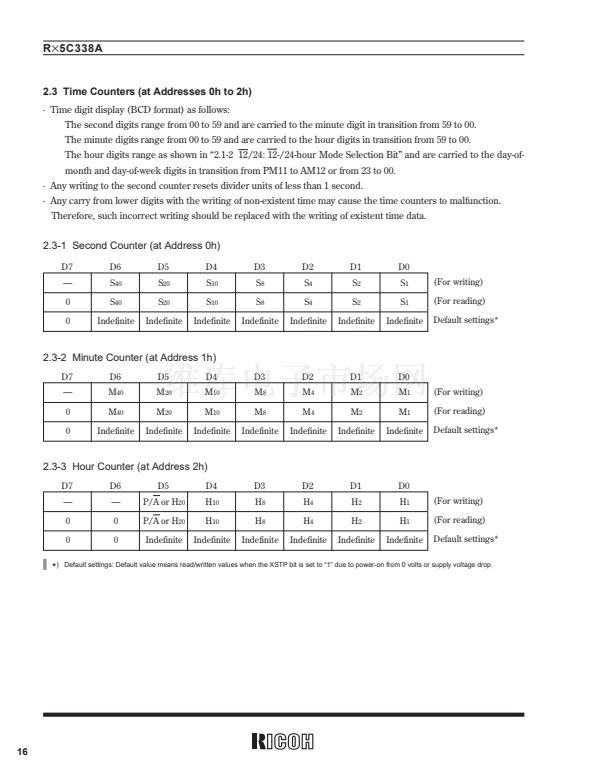
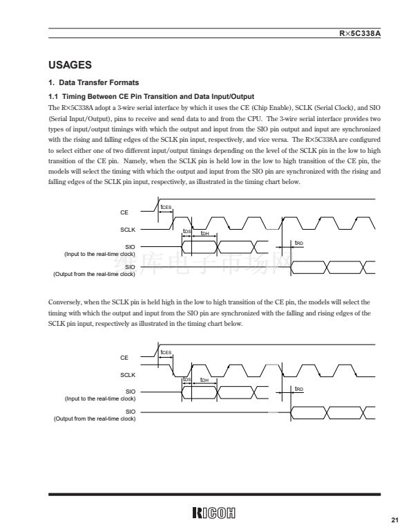
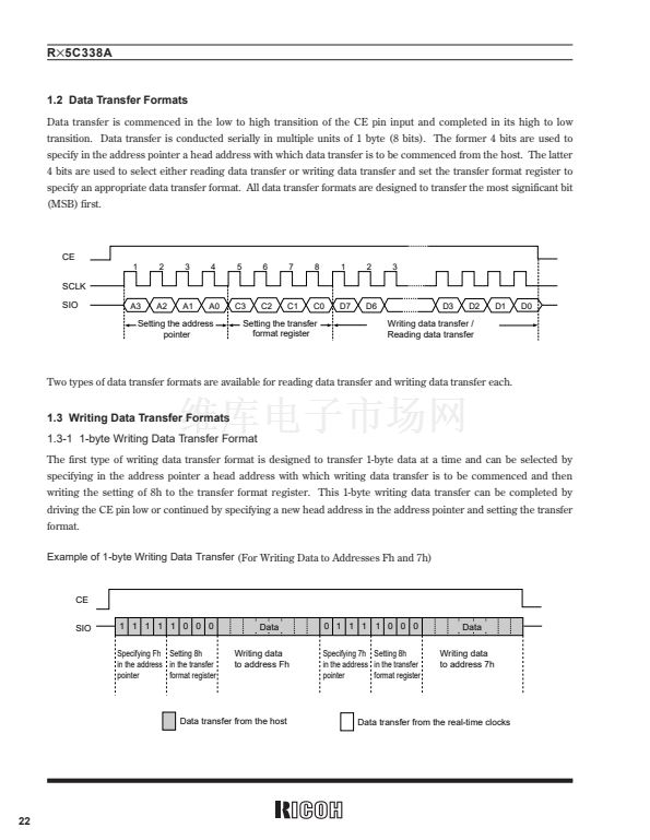
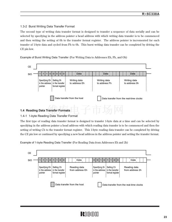
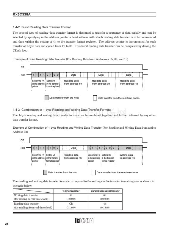
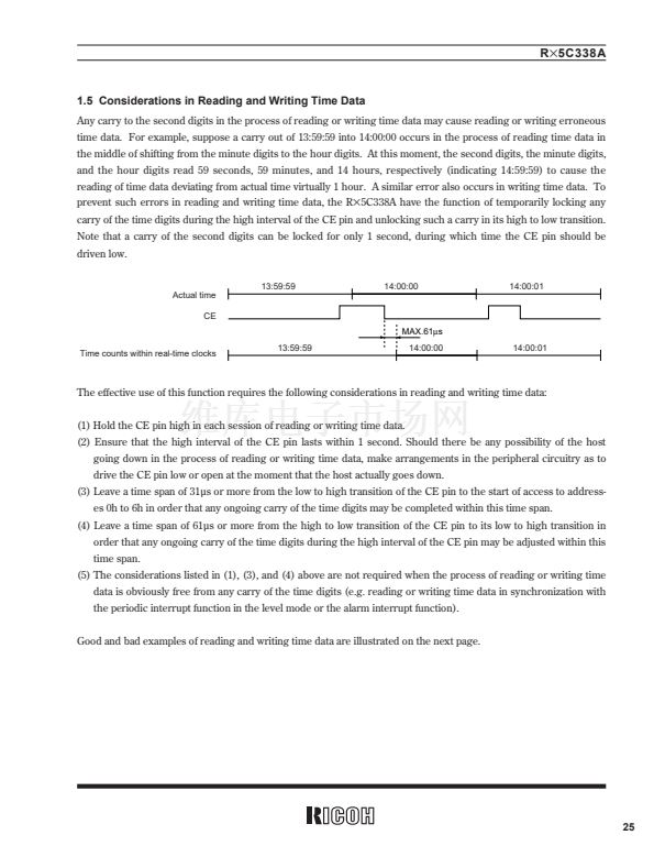
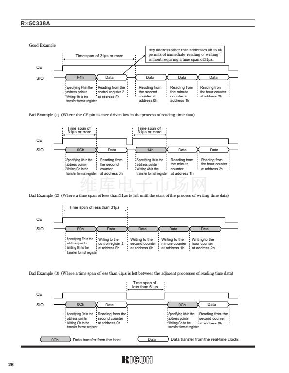
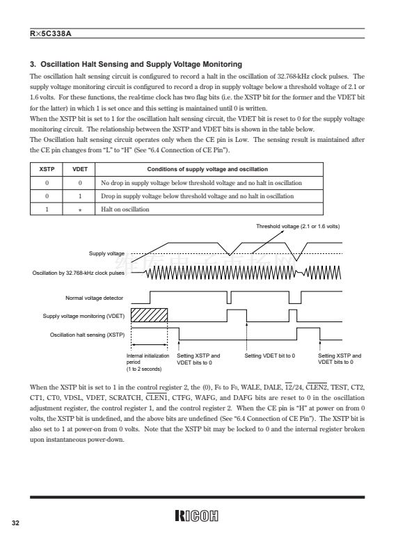
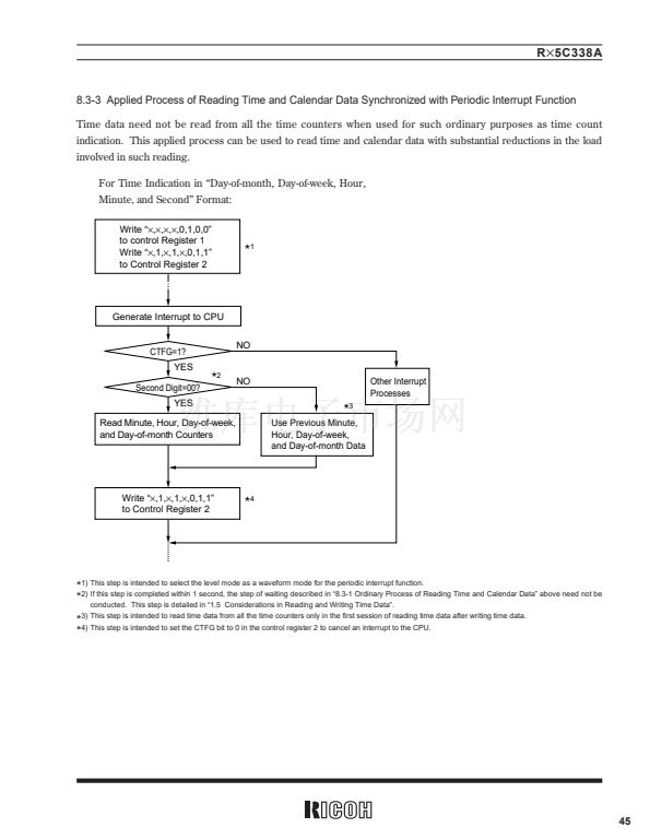
R
脳
5C338A
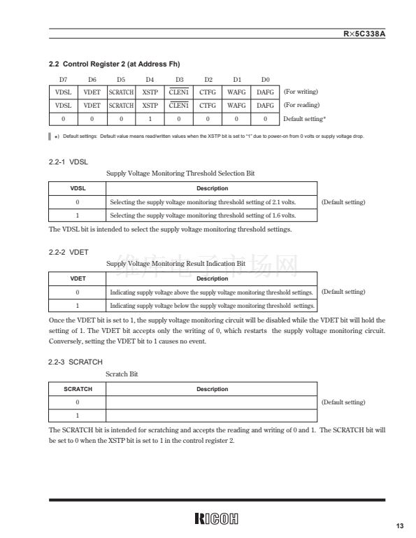
2.2 Control Register 2 (at Address Fh)
D7
VDSL
VDSL
0
D6
VDET
VDET
0
D5
SCRATCH
SCRATCH
0
D4
XSTP
XSTP
1
D3
CLEN1
CLEN1
0
D2
CTFG
CTFG
0
D1
WAFG
WAFG
0
D0
DAFG
DAFG
0
(For writing)
(For reading)
Default setting*
*
)
Default settings: Default value means read/written values when the XSTP bit is set to 鈥?鈥?due to power-on from 0 volts or supply voltage drop.
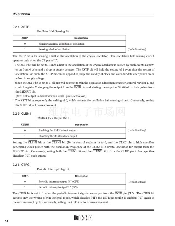
2.2-1 VDSL
Supply Voltage Monitoring Threshold Selection Bit
VDSL
Description
0
1
Selecting the supply voltage monitoring threshold setting of 2.1 volts.
Selecting the supply voltage monitoring threshold setting of 1.6 volts.
(Default setting)
The VDSL bit is intended to select the supply voltage monitoring threshold settings.
2.2-2 VDET
Supply Voltage Monitoring Result Indication Bit
VDET
Description
0
1
Indicating supply voltage above the supply voltage monitoring threshold settings.
Indicating supply voltage below the supply voltage monitoring threshold settings.
(Default setting)
Once the VDET bit is set to 1, the supply voltage monitoring circuit will be disabled while the VDET bit will hold the
setting of 1. The VDET bit accepts only the writing of 0, which restarts the supply voltage monitoring circuit.
Conversely, setting the VDET bit to 1 causes no event.
2.2-3 SCRATCH
Scratch Bit
SCRATCH
Description
0
1
(Default setting)
The SCRATCH bit is intended for scratching and accepts the reading and writing of 0 and 1. The SCRATCH bit will
be set to 0 when the XSTP bit is set to 1 in the control register 2.
13


 1
1
 2
2
 3
3
 4
4
 5
5
 6
6
 7
7
 8
8
 9
9
 10
10
 11
11
 12
12
 13
13
 14
14
 15
15
 16
16
 17
17
 18
18
 19
19
 20
20
 21
21
 22
22
 23
23
 24
24
 25
25
 26
26
 27
27
 28
28
 29
29
 30
30
 31
31
 32
32
 33
33
 34
34
 35
35
 36
36
 37
37
 38
38
 39
39
 40
40
 41
41
 42
42
 43
43
 44
44
 45
45
 46
46
 47
47
 48
48
 49
49
 50
50
 51
51
 52
52
