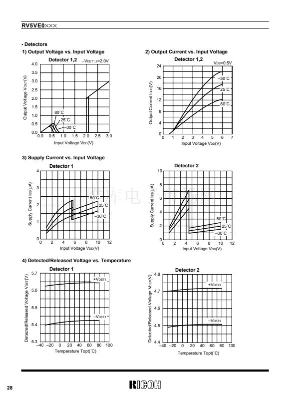
level. The output of Voltage Detector 1 is Nch Open Drain Output.
鈥?/div>
Voltage Detector 1 can be set as follows by optional mask:
1. ON/OFF Control of Voltage Detector 1.
2. Output of Voltage Detector 1 at the detection can be set at 鈥淟鈥?level or 鈥淗鈥?level.
3. Output of Voltage Detector 1 at OFF can be set at 鈥淟鈥?level or 鈥淗鈥?level.
4. Sense Pins of Voltage Detectors 1, 2 can be connected to Output R
OUT1
, R
OUT2
, R
OUT3
, R
OUT4
of Voltage
Regulators or V
DD
within the IC.
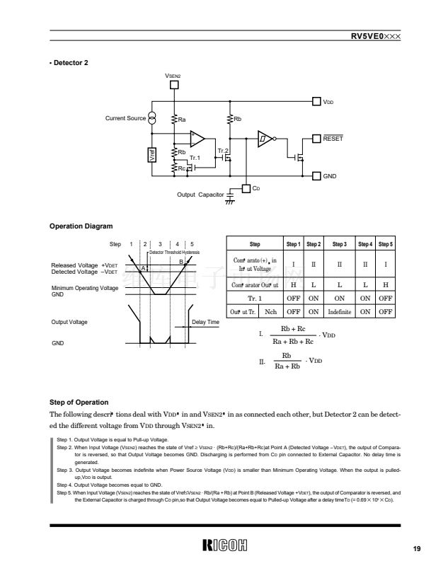
4. Voltage Detector 2
鈥?/div>
When Voltage Detector 2 detects the lowering of V
SEN2
, the level of the output of Voltage Detector 2 becomes 鈥淟鈥?/div>
level. The output of Voltage Detector 2 is Nch Open Drain Output.
鈥?/div>
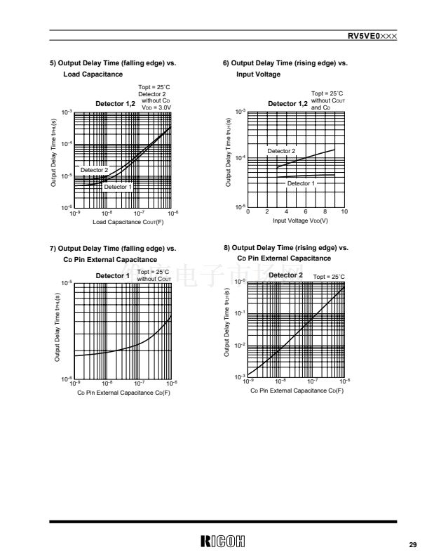
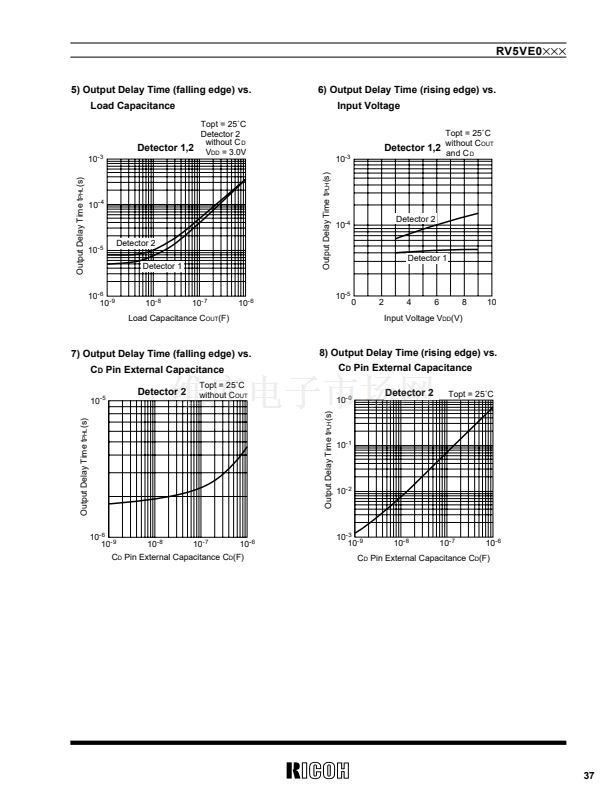
Voltage Detector 2 can set Reset Delay Time. Delay Time can be set in accordance with the capacitance C
D
of
External Capacitor as shown on the following pages.
鈥?/div>
Voltage detector 2 can be set as follows by optional mask:
1. ON/OFF Control of Voltage Detector 2.
2. Output of Voltage Detector 2 at the detection can be set at 鈥淟鈥?level or 鈥淗鈥?level.
3. Output of Voltage Detector 2 at OFF can be set at 鈥淟鈥?level or 鈥淗鈥?level.
4. Sense Pins of Voltage Detectors 2 can be connected to Output R
OUT1
, R
OUT2
, R
OUT3
, R
OUT4
of Voltage
Regulators or V
DD
within the IC.
5


 1
1
 2
2
 3
3
 4
4
 5
5
 6
6
 7
7
 8
8
 9
9
 10
10
 11
11
 12
12
 13
13
 14
14
 15
15
 16
16
 17
17
 18
18
 19
19
 20
20
 21
21
 22
22
 23
23
 24
24
 25
25
 26
26
 27
27
 28
28
 29
29
 30
30
 31
31
 32
32
 33
33
 34
34
 35
35
 36
36
 37
37
 38
38
 39
39
 40
40
 41
41
 42
42
 43
43
 44
44
 45
45
 46
46
 47
47
 48
48
 49
49
