鈥?/div>
RV5VE001
脳
(Standard ICs)
Pin No.
Symbol
Description
1
2
3
4
5
6
7
8
9
10
11
R
OUT
4
V
SEN
2
C
D
RESET
D
OUT
R
OUT
1
I
BC
1
GND
I
BC
2
R
OUT
2
CSW1
Output Pin for Voltage Regulator 4.
Sense Pin for Voltage Detector 2.
Pin for External Capacitor for Delay Time Setting of Voltage Detector 2.
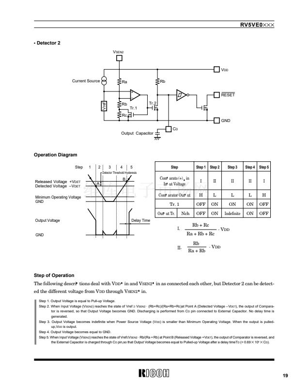
Output Pin of Voltage Detector 2. Nch Open Drain Output. 鈥淟鈥?Outputat Detection.
Output Pin of Voltage Detector 1. Nch Open Drain Output. 鈥淟鈥?Output at Detection.
Output Pin of Voltage Regulator 1. Connected to Collector of PNP Transistor.
Connected to Base of External PNP Transistor for Voltage Regulator 1 and controls Base Current.
Ground Pin.
Connected to Base of External PNP Transistor for Voltage Regulator 2 and controls Base Current.
Output Pin of Voltage Regulator 2. Connected to Collector of PNP Transistor.
Control Switch Input Pin for turning Voltage Regulator 1 ON/OFF.
Input level for this Input Pin is Active 鈥淗鈥?.
Control Switch Input Pin for turning Voltage Regulator 2 ON/OFF.
Input level for this Input Pin is Active 鈥淗鈥?/div>
Control Switch Input Pin for turning Voltage Regulator 3 ON/OFF.
Input level for this Input Pin is Active 鈥淗鈥?.
12
CSW2
13
CSW3
14
15
16
V
SEN
1
R
OUT
3
V
DD
Sense Pin of Voltage Detector 1.
Output Pin of Voltage Regulator 3.
V
DD
Pin.
鈥?/div>
RV5VE0
脳脳脳
(Optional Mask Version ICs)
Pin No.
Symbol
Description
2
11
12
13
14
To be
named
by User
5 Pins Nos. 2, 11, 12, 13 and 14 can be designated as Input Pins by User's
choice. Refer to Optional Mask Version Guide.
Pins other than the above 5 Pins can be selected from the same pins as those
used in R
脳
5VE001
脳
(Standard ICs)
3


 1
1
 2
2
 3
3
 4
4
 5
5
 6
6
 7
7
 8
8
 9
9
 10
10
 11
11
 12
12
 13
13
 14
14
 15
15
 16
16
 17
17
 18
18
 19
19
 20
20
 21
21
 22
22
 23
23
 24
24
 25
25
 26
26
 27
27
 28
28
 29
29
 30
30
 31
31
 32
32
 33
33
 34
34
 35
35
 36
36
 37
37
 38
38
 39
39
 40
40
 41
41
 42
42
 43
43
 44
44
 45
45
 46
46
 47
47
 48
48
 49
49
