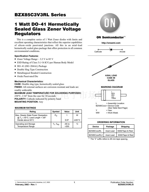
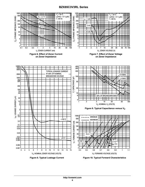
BZX85C3V3RL Series
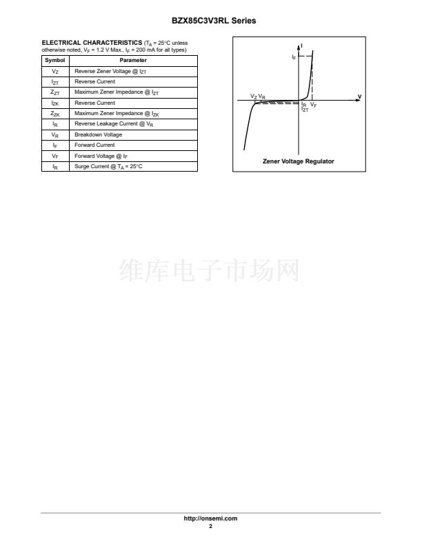
ELECTRICAL CHARACTERISTICS
(T
A
= 25擄C unless otherwise noted, V
F
= 1.2 V Max., I
F
= 200 mA for all types)
Zener Voltage
(Notes 2 and 3)
Device
(Note 1)
BZX85C3V3RL
BZX85C3V6RL
BZX85C3V9RL
BZX85C4V3RL
BZX85C4V7RL
BZX85C5V1RL
BZX85C5V6RL
BZX85C6V2RL
BZX85C6V8RL
BZX85C7V5RL
BZX85C8V2RL
BZX85C9V1RL
BZX85C10RL
BZX85C12RL
BZX85C13RL
BZX85C15RL
BZX85C16RL
BZX85C18RL
BZX85C22RL
BZX85C24RL
BZX85C27RL
BZX85C30RL
BZX85C33RL
BZX85C36RL
BZX85C43RL
BZX85C47RL
BZX85C62RL
BZX85C75RL
BZX85C82RL
Device
Marking
BZX85C3V3
BZX85C3V6
BZX85C3V9
BZX85C4V3
BZX85C4V7
BZX85C5V1
BZX85C5V6
BZX85C6V2
BZX85C6V8
BZX85C7V5
BZX85C8V2
BZX85C9V1
BZX85C10
BZX85C12
BZX85C13
BZX85C15
BZX85C16
BZX85C18
BZX85C22
BZX85C24
BZX85C27
BZX85C30
BZX85C33
BZX85C36
BZX85C43
BZX85C47
BZX85C62
BZX85C75
BZX85C82
V
Z
(Volts)
Min
3.1
3.4
3.7
4.0
4.4
4.8
5.2
5.8
6.4
7.0
7.7
8.5
9.4
11.4
12.4
13.8
15.3
16.8
20.8
22.8
25.1
28
31
34
40
44
58
70
77
Nom
3.3
3.6
3.9
4.3
4.7
5.1
5.6
6.2
6.8
7.45
8.2
9.05
10
12.05
13.25
14.7
16.2
17.95
22.05
24.2
27
30
33
36
43
47
62
75
82
Max
3.5
3.8
4.1
4.6
5.0
5.4
6.0
6.6
7.2
7.9
8.7
9.6
10.6
12.7
14.1
15.6
17.1
19.1
23.3
25.6
28.9
32
35
38
46
50
66
80
87
@ I
ZT
mA
80
60
60
50
45
45
45
35
35
35
25
25
25
20
20
15
15
15
10
10
8
8
8
8
6
4
4
4
2.7
Zener Impedance
(Note 4)
Z
ZT
@ I
ZT
W
20
15
15
13
13
10
7
4
3.5
3
5
5
7
9
10
15
15
20
25
25
30
30
35
40
50
90
125
150
200
Z
ZK
@ I
ZK
W
400
500
500
500
600
500
400
300
300
200
200
200
200
350
400
500
500
500
600
600
750
1000
1000
1000
1000
1500
2000
2000
3000
mA
1
1
1
1
1
1
1
1
1
0.5
0.5
0.5
0.5
0.5
0.5
0.5
0.5
0.5
0.5
0.5
0.25
0.25
0.25
0.25
0.25
0.25
0.25
0.25
0.25
Leakage Current
I
R
@ V
R
碌A(chǔ)
Max
1
1
1
1
1.5
2
2
3
4
4.5
5
6.5
7
8.4
9.1
10.5
11
12.5
15.5
17
19
21
23
25
30
33
43
51
56
Volts
60
30
5
3
3
1
1
1
1
1
1
1
0.5
0.5
0.5
0.5
0.5
0.5
0.5
0.5
0.5
0.5
0.5
0.5
0.5
0.5
0.5
0.5
0.5
I
R
(Note 5)
mA
1380
1260
1190
1070
970
890
810
730
660
605
550
500
454
380
344
304
285
250
205
190
170
150
135
125
110
95
70
60
55
1.
TOLERANCE AND TYPE NUMBER DESIGNATION
The type numbers listed have zener voltage min/max limits as shown and have a standard tolerance on the nominal zener voltage of
鹵5%.
2.
AVAILABILITY OF SPECIAL DIODES
For detailed information on price, availability and delivery of nominal zener voltages between the voltages shown and tighter voltage
tolerances, contact your nearest ON Semiconductor representative.
3.
ZENER VOLTAGE (V
Z
) MEASUREMENT
V
Z
measured after the test current has been applied to 40
鹵10
msec, while maintaining the lead temperature (T
L
) at 30擄C
鹵1擄C,
3/8鈥?from
the diode body.
4.
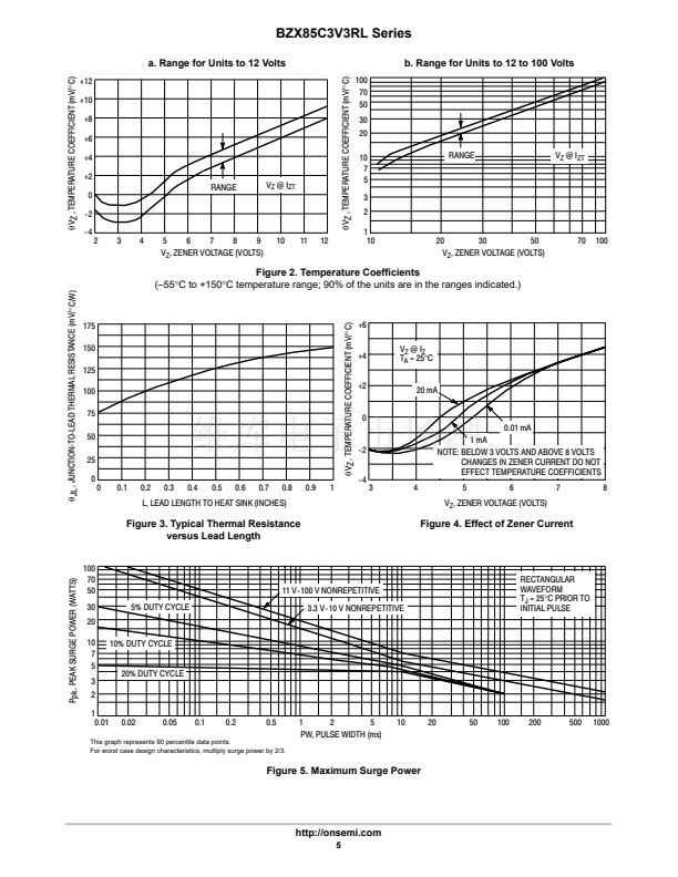
ZENER IMPEDANCE (Z
Z
) DERIVATION
The zener impedance is derived from 1 kHz cycle AC voltage, which results when an AC current having an rms value equal to 10% of the
DC zener current (I
ZT
or I
ZK
) is superimposed on I
ZT
or I
ZK
.
5.
SURGE CURRENT (I
R
) NON鈥揜EPETITIVE
The rating listed in the electrical characteristics table is maximum peak, non鈥搑epetitive, reverse surge current of 1/2 square wave or eqivalent
sine wave pulse of 1/120 second duration superimposed on the test current, I
ZT
. However, actual device capability is as described in Figure
5 of the General Data 鈥?DO鈥?1 Glass.
http://onsemi.com
3


 1
1
 2
2
 3
3
 4
4
 5
5
 6
6
 7
7
 8
8
