鈭?/div>
S
I
I
S
A
DESCRIPTION
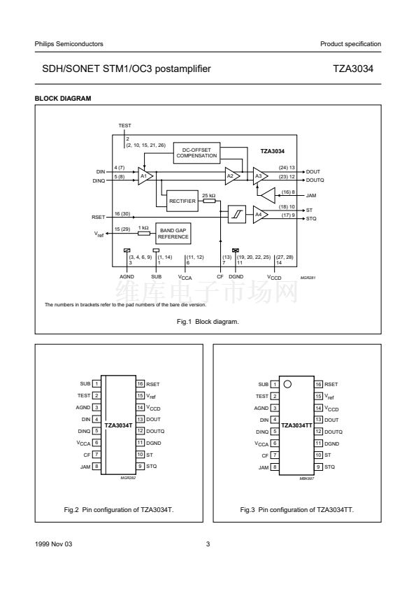
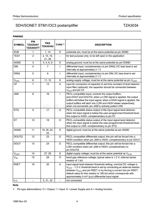
TZA3034
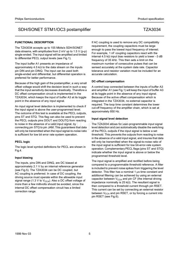
substrate pin; must be at the same potential as pin AGND
for test purpose only; to be left open in the application
analog ground; must be at the same potential as pin DGND
differential input; complementary to pin DINQ; DC bias level is set
internally at approximately 2.1 V
differential input; complementary to pin DIN; DC bias level is set
internally at approximately 2.1 V
analog supply voltage; must be at the same potential as pin V
CCD
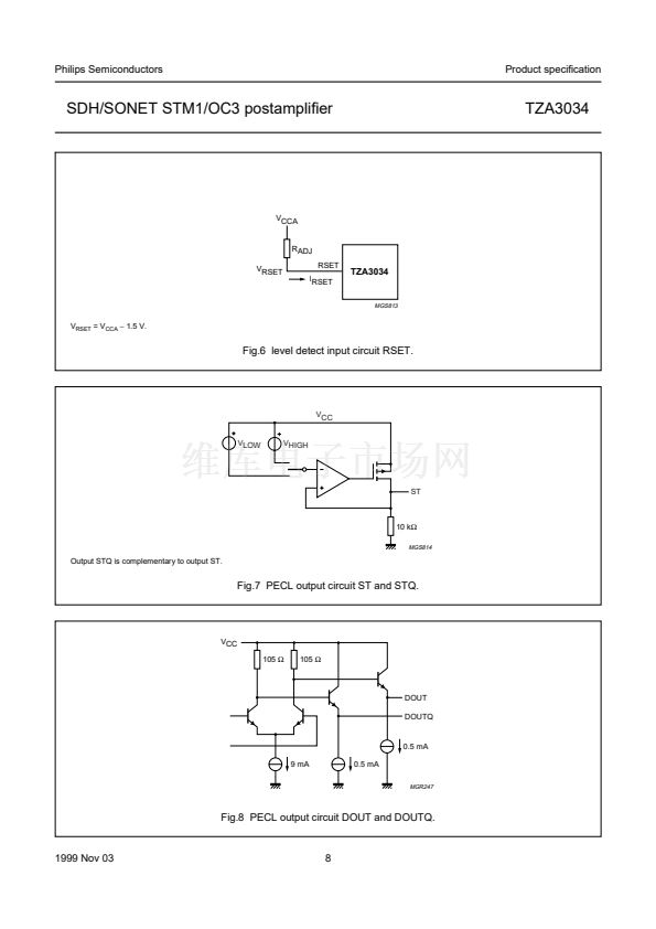
input for connection of capacitor to set time constant of level detector
input 鏗乴ter (optional); the capacitor should be connected between
V
CCA
and pin CF
PECL-compatible input; controls the output buffers,
pins DOUT and DOUTQ; when a LOW signal is applied, the output
buffers will follow the input signal; when a HIGH signal is applied, the
output buffers will latch into LOW and HIGH states respectively;
when not connected, pin JAM is actively pulled LOW
PECL-compatible status output of the input signal level detector;
when the input signal is below the user-programmed threshold level,
this output is HIGH; complementary to pin ST
PECL-compatible status output of the input signal level detector;
when the input signal is below the user-programmed threshold level,
this output is LOW; complementary to pin STQ
digital ground; must be at the same potential as pin AGND
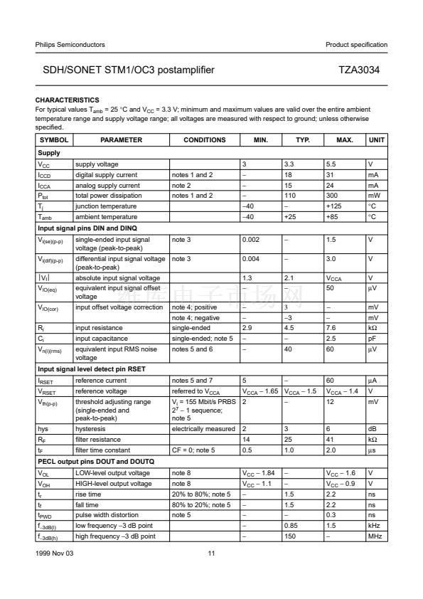
PECL-compatible differential output; this pin will be forced into a
HIGH condition when pin JAM is HIGH; complementary to pin DOUT
PECL-compatible differential output; this pin will be forced into a
LOW condition when pin JAM is HIGH; complementary to
pin DOUTQ
digital supply voltage; must be at the same potential as V
CCA
band gap reference voltage; typical value is 1.2 V; internal series
resistor of 1 k鈩?/div>
input signal level detector threshold setting; nominal DC voltage is
V
CCA
鈭?/div>
1.5 V; threshold level is set by connecting an external resistor
between V
CCA
and pin RSET or by forcing a current into pin RSET;
default value for this resistor is 180 k鈩?which corresponds with
approximately 4 mV (p-p) differential input signal
not connected
JAM
8
16
I
STQ
9
17
O
ST
10
18
O
DGND
DOUTQ
DOUT
11
12
13
19, 20, 22,
25
23
24
S
O
O
V
CCD
V
ref
RSET
14
15
16
27, 28
29
30
S
O
A
n.c.
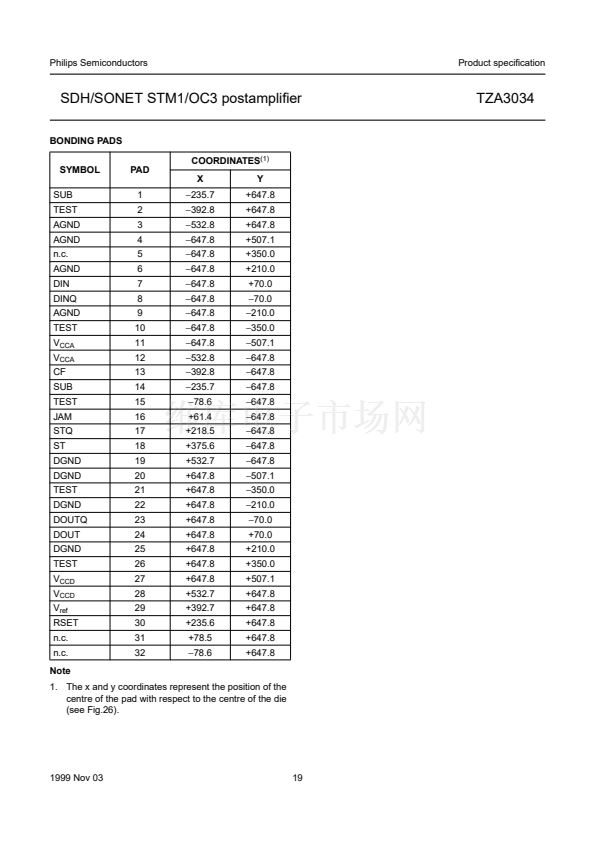
Note
鈭?/div>
5, 31, 32
鈭?/div>
1. Pin type abbreviations: O = Output, I = Input, S = power Supply and A = Analog function.
1999 Nov 03
4


 1
1
 2
2
 3
3
 4
4
 5
5
 6
6
 7
7
 8
8
 9
9
 10
10
 11
11
 12
12
 13
13
 14
14
 15
15
 16
16
 17
17
 18
18
 19
19
 20
20
 21
21
 22
22
 23
23
 24
24
 25
25
 26
26
 27
27
 28
28
