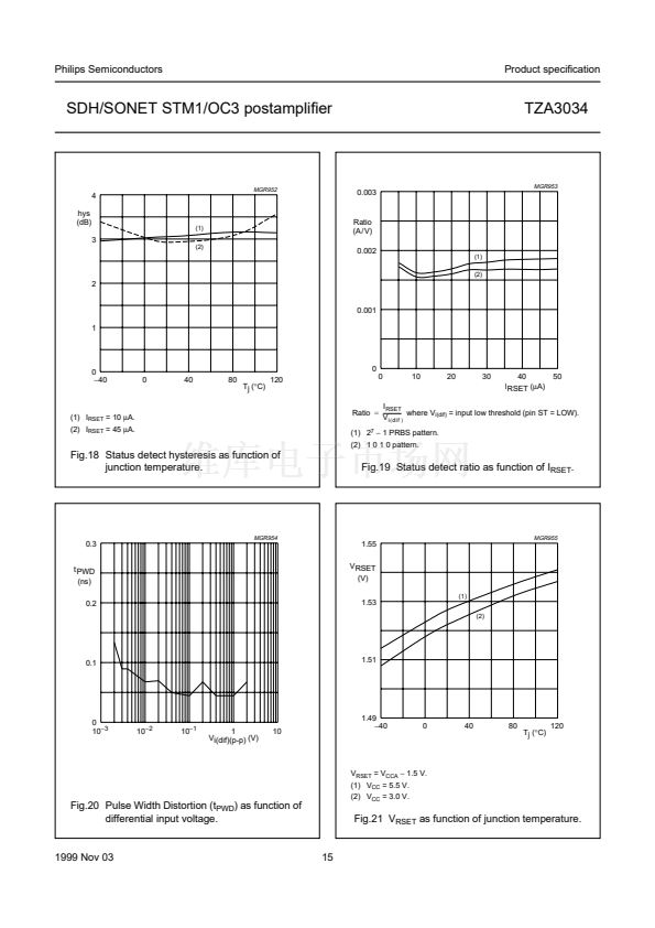
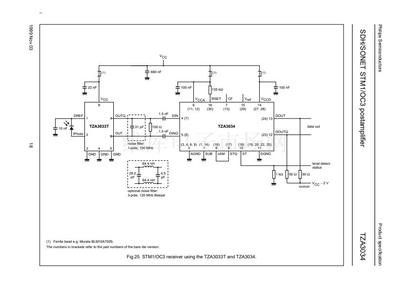
鈭?/div>
鈭?0
V
V
pF
pF
pF
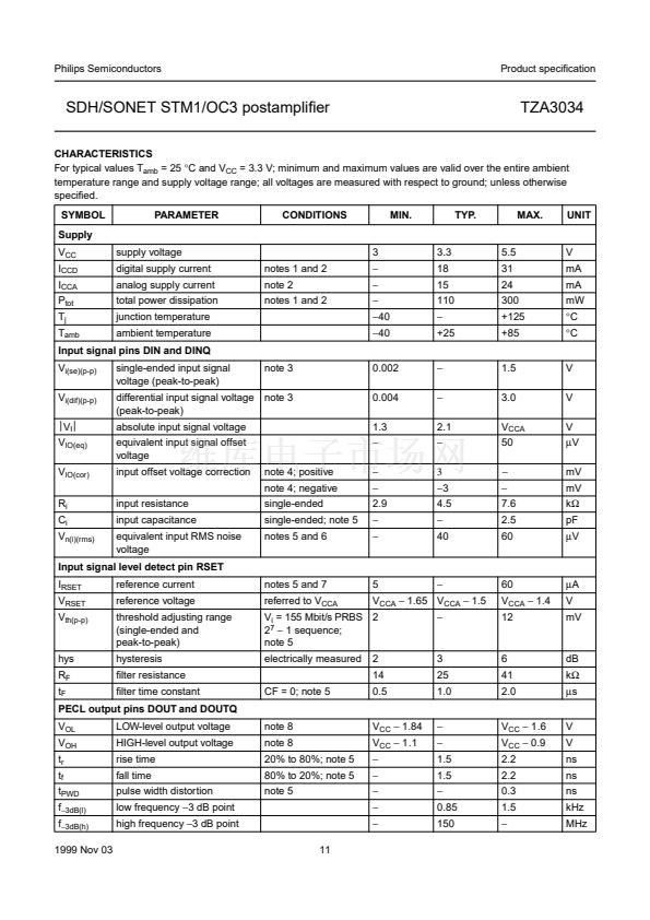
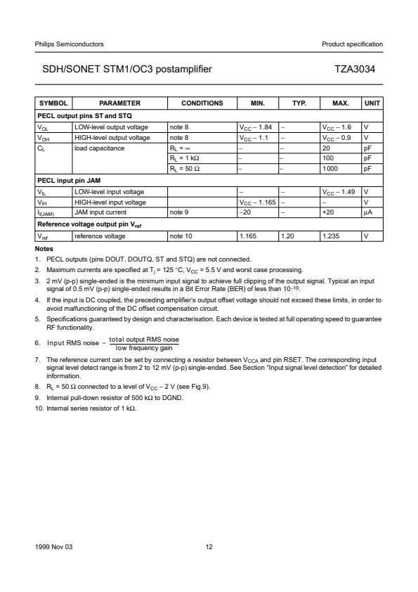
Reference voltage output pin V
ref
V
ref
Notes
1. PECL outputs (pins DOUT, DOUTQ, ST and STQ) are not connected.
2. Maximum currents are specified at T
j
= 125
擄C,
V
CC
= 5.5 V and worst case processing.
3. 2 mV (p-p) single-ended is the minimum input signal to achieve full clipping of the output signal. Typical an input
signal of 0.5 mV (p-p) single-ended results in a Bit Error Rate (BER) of less than 10
鈭?0
.
4. If the input is DC coupled, the preceding amplifier鈥檚 output offset voltage should not exceed these limits, in order to
avoid malfunctioning of the DC offset compensation circuit.
5. Specifications guaranteed by design and characterisation. Each device is tested at full operating speed to guarantee
RF functionality.
6.
total output RMS noise
Input RMS noise
=
--------------------------------------------------------------
-
low frequency gain
reference voltage
note 10
1.165
1.20
1.235
V
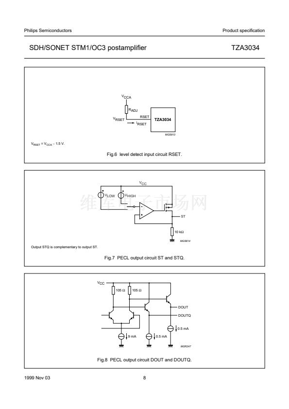
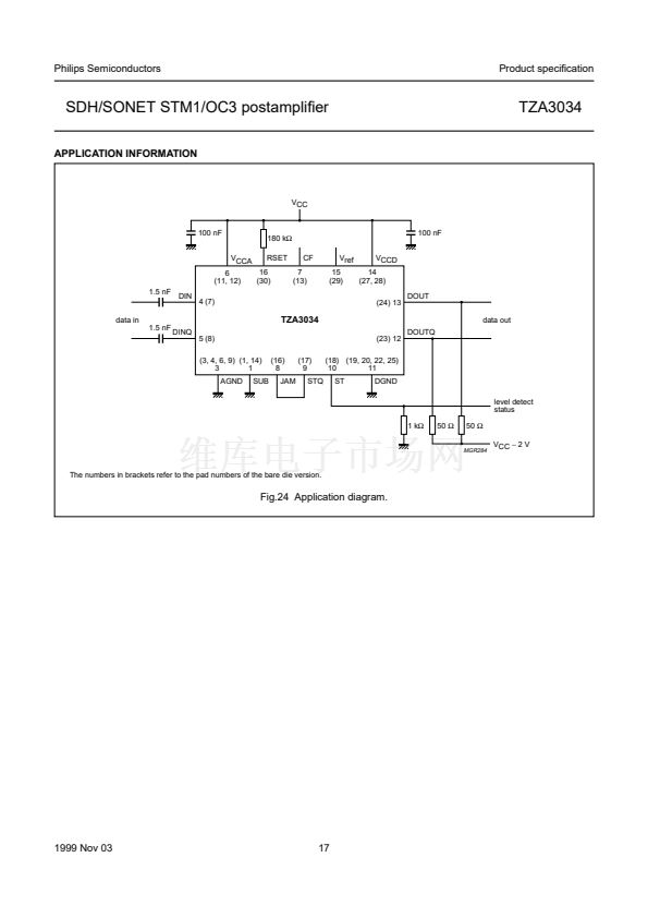
7. The reference current can be set by connecting a resistor between V
CCA
and pin RSET. The corresponding input
signal level detect range is from 2 to 12 mV (p-p) single-ended. See Section 鈥淚nput signal level detection鈥?for detailed
information.
8. R
L
= 50
鈩?/div>
connected to a level of V
CC
鈭?/div>
2 V (see Fig.9).
9. Internal pull-down resistor of 500 k鈩?to DGND.
10. Internal series resistor of 1 k鈩?
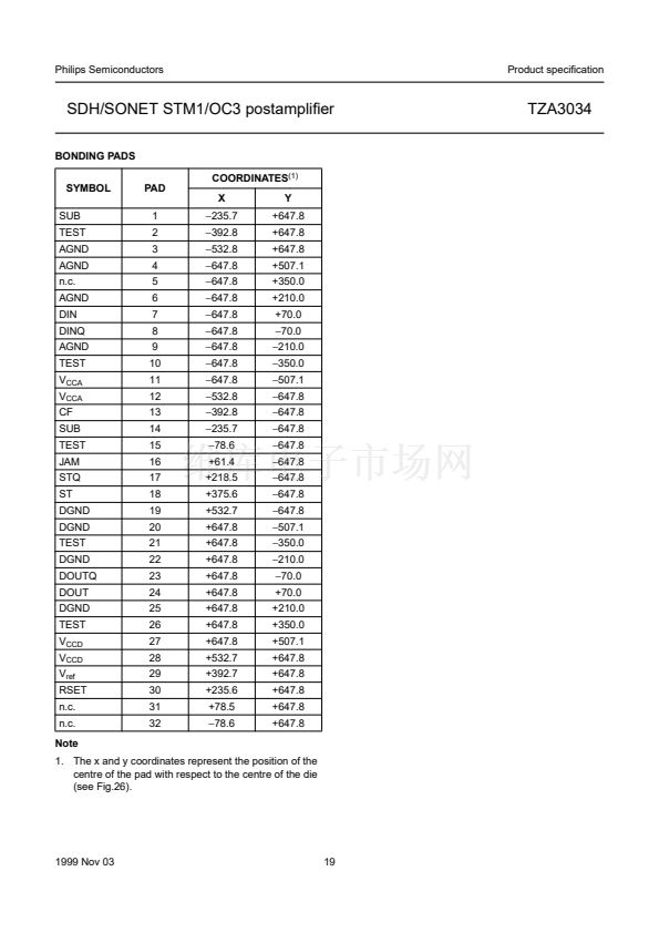
1999 Nov 03
12


 1
1
 2
2
 3
3
 4
4
 5
5
 6
6
 7
7
 8
8
 9
9
 10
10
 11
11
 12
12
 13
13
 14
14
 15
15
 16
16
 17
17
 18
18
 19
19
 20
20
 21
21
 22
22
 23
23
 24
24
 25
25
 26
26
 27
27
 28
28
