鈭?/div>
2
鈭?.5
PARAMETER
MIN.
鈭?.5
TZA3034
MAX.
+6
V
CC
+ 0.5
V
CC
+ 0.5
+3.2
V
V
V
V
UNIT
mA
mA
mA
mA
mW
擄C
擄C
擄C
This device is ESD sensitive and should be handled with care. Precautions should be taken to avoid damage through
electrostatic discharge. This is particularly important during assembly and handling of the bare die. Additional safety can
be obtained by bonding the V
CC
and GND pads first, the remaining pads may then be bonded to their external
connections in any order.
THERMAL CHARACTERISTICS
SYMBOL
R
th(j-a)
PARAMETER
SO16 package
TSSOP16 package
Note
1. Thermal resistance from junction to ambient is determined with the IC soldered on a standard single-sided
57
脳
57
脳
1.6 mm FR4 epoxy printed-circuit board with 35
碌m
thick copper traces. The measurements are performed
in still air.
CONDITION
VALUE
115
150
UNIT
K/W
K/W
thermal resistance from junction to ambient note 1
1999 Nov 03
10


 1
1
 2
2
 3
3
 4
4
 5
5
 6
6
 7
7
 8
8
 9
9
 10
10
 11
11
 12
12
 13
13
 14
14
 15
15
 16
16
 17
17
 18
18
 19
19
 20
20
 21
21
 22
22
 23
23
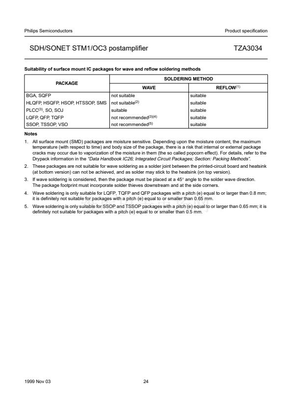 24
24
 25
25
 26
26
 27
27
 28
28
