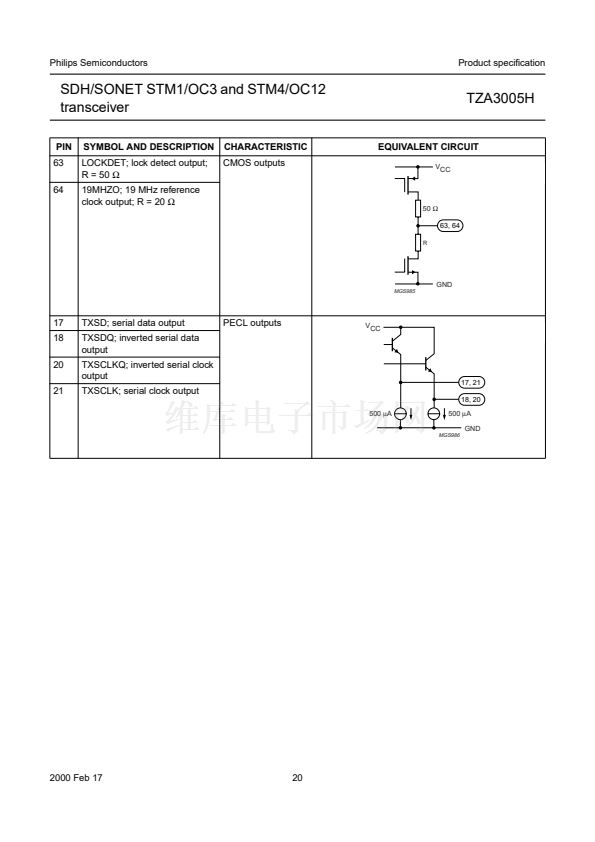
Philips Semiconductors
Product speci鏗乧ation
SDH/SONET STM1/OC3 and STM4/OC12
transceiver
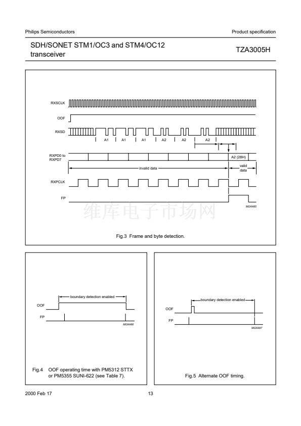
Other operating modes
D
IAGNOSTIC LOOPBACK
A transmitter-to-receiver loopback mode is available for
diagnostic purposes. When DLEN is LOW, the differential
serial clock and data from the transmitter parallel-to-serial
block continue to be routed to transmitter outputs, but are
also routed to the receiver serial-to-parallel block instead
of the receiver input signals from pins RXSD/RXSDQ and
RXSCLK/RXSCLKQ.
L
INE LOOPBACK
A receiver-to-transmitter loopback mode is available for
line testing purposes. When LLEN is LOW, the receiver
input signals (RXSD/RXSDQ and RXSCLK/RXSCLKQ)
are routed, after retiming, to the transmitter output buffers.
The receiver clock and data are also routed to the
serial-to-parallel block.
L
OOP TIMING
In loop timing mode, the transmitter section is clocked by
the receiver input clock (RXSCLK) instead of by the
internal clock synthesizer. SYNCLKDIV is now derived
from RXSCLK so that it can be used to clock upstream
transmitter logic. Loop timing is enabled by setting pins
ALTPIN, TEST1, TEST2 and TEST3 (see Table 6). After
activating the loop timing mode, the receiver clock must be
synchronized to the transmitter input data
(TXPD0 to TXPD7) by activating master reset (MRST).
In loop timing mode, the internal clock synthesizer is still
used to generate the 19MHz output clock signal on
pin 19MHZO.
S
QUELCHED CLOCK OPERATION
TZA3005H
Some clock recovery devices force their recovered output
clock to zero if a loss of input signal is detected. If this
happens, the SDTTL or SDPECL signals are inactive and
no clock signal is present at pins RXSCLK and RXSCLKQ.
If no clock signal is present at pins RXSCLK/RXSCLKQ,
there is no RXPCLK signal. This may not be suitable for
some applications, in which case, the TZA3005H can be
set to squelched clock operation by setting pins ALTPIN,
TEST1, TEST2 and TEST3 as shown in Table 6.
In squelched clock operation, receiver timing is performed
by a part of the internal clock synthesizer which normally
only provides transmitter timing. This produces a RXPCLK
clock signal when either SDTTL or SDPECL is inactive. If
either SDTTL or SDPECL is inactive in squelched clock
operation, it is equivalent to normal operation. During a
transition from normal operation to squelched clock
operation, the RXPCLK clock cycle exhibits a once-only
random shortening.
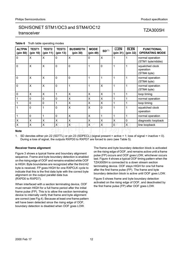
Table 6 shows that the same operating mode can be
selected at different settings of the control inputs.
If ALTPIN = 0, the STM4 nibble mode is not available, but
is used for squelched clock operation. If ALTPIN = 1, all
operating modes are available, including STM4 nibble
mode.
2000 Feb 17
11


 1
1
 2
2
 3
3
 4
4
 5
5
 6
6
 7
7
 8
8
 9
9
 10
10
 11
11
 12
12
 13
13
 14
14
 15
15
 16
16
 17
17
 18
18
 19
19
 20
20
 21
21
 22
22
 23
23
 24
24
 25
25
 26
26
 27
27
 28
28
