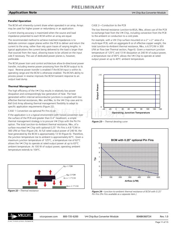
The thermal resistance of the PCB to the surrounding environment in
proximity to V鈥 Chips may be reduced by low profile heat sinks surface
mounted to the PCB.The PCB may also be coupled to a cold plate by low
thermal resistance standoff elements as a means of achieving effective
cooling for an array of V鈥 Chips, without a direct interface to their case.
CASE 3鈥擟ombined direct convection to the air and conduction to the PCB.
Parallel use of the V鈥 Chip internal thermal resistances (including Junction-
to-Case and Junction-to-BGA) in series with external thermal resistances
provides an efficient thermal management strategy as it reduces total
thermal resistance. This may be readily estimated as the parallel network of
two pairs of series configured resistors.
V鈥 Chip Bus Converter Module
V鈥 Chip Bus Converter Level 1 DC Behavioral Model for 48 V to 6 V, 240 W
I
OUT
R
OUT
5.5 m鈩?/div>
+
1/8 鈥?Iout
+
V
鈥?/div>
I
1/8 鈥?Vin
V
IN
I
Q
47 mA
+
鈥?/div>
K
+
V
OUT
鈥?/div>
鈥?/div>
漏
鈥?/div>
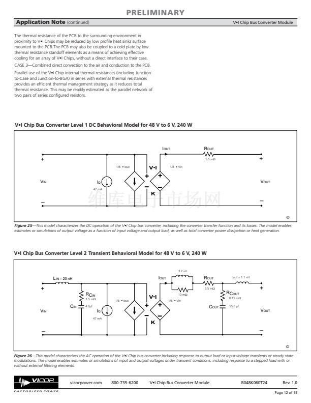
Figure 25鈥擳his
model characterizes the DC operation of the V鈥 Chip bus converter, including the converter transfer function and its losses. The model enables
estimates or simulations of output voltage as a function of input voltage and output load, as well as total converter power dissipation or heat generation.
V鈥 Chip Bus Converter Level 2 Transient Behavioral Model for 48 V to 6 V, 240 W
3.2 nH
L
IN
= 20 nH
I
OUT
R
OUT
5.5 m鈩?/div>
Lout = 1.1 nH
+
RC
IN
1.5 m鈩?/div>
1/8 鈥?Iout
V
鈥?/div>
I
10 m鈩?/div>
RC
OUT
0.15 m鈩?/div>
+
C
IN
V
IN
4.0碌F
I
Q
47 mA
+
鈥?/div>
K
+
鈥?/div>
1/8 鈥?Vin
C
OUT
55.0 碌F
V
OUT
鈥?/div>
鈥?/div>
漏
Figure 26鈥擳his
model characterizes the AC operation of the V鈥 Chip bus converter including response to output load or input voltage transients or steady state
modulations. The model enables estimates or simulations of input and output voltages under transient conditions, including response to a stepped load with or


 1
1
 2
2
 3
3
 4
4
 5
5
 6
6
 7
7
 8
8
 9
9
 10
10
 11
11
 12
12
 13
13
 14
14
 15
15
