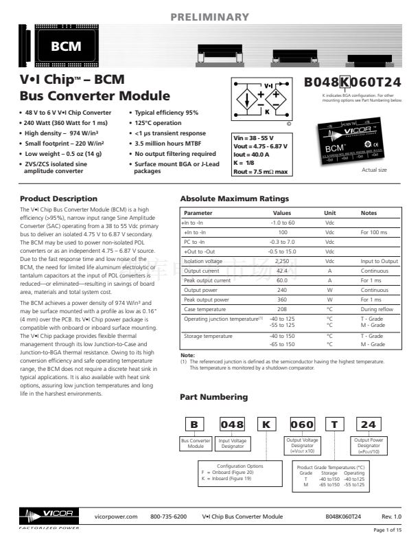
PRELIMINARY
Application Note
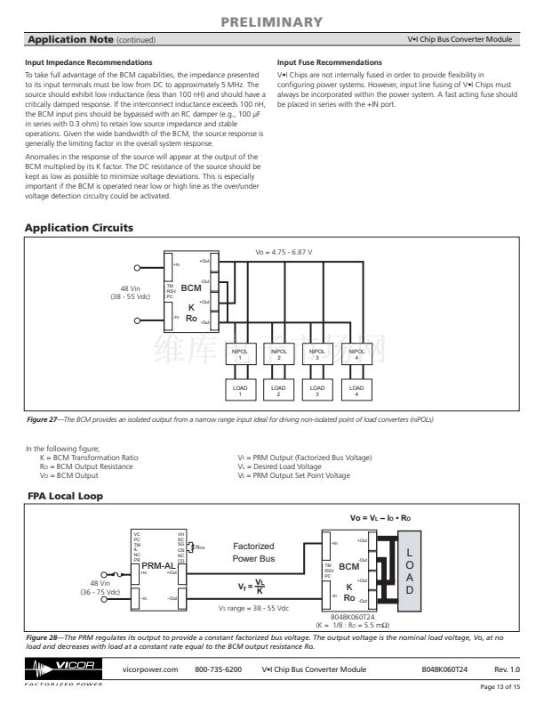
Parallel Operation
The BCM will inherently current share when operated in an array. Arrays
may be used for higher power or redundancy in an application.
Current sharing accuracy is maximized when the source and load
impedance presented to each BCM within an array are equal.
The recommended method to achieve matched impedances is to
dedicate common copper planes within the PCB to deliver and return the
current to the array, rather than rely upon traces of varying lengths. In
typical applications the current being delivered to the load is larger than
that sourced from the input, allowing traces to be utilized on the input
side if necessary. The use of dedicated power planes is, however,
preferable.
The BCM power train and control architecture allow bi-directional power
transfer, including reverse power processing from the BCM output to its
input. Reverse power transfer is enabled if the BCM input is within its
operating range and the BCM is otherwise enabled. The BCM鈥檚 ability to
process power in reverse improves the BCM transient response to an
output load dump.
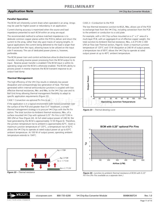
Thermal Management
The high efficiency of the V鈥 Chip results in relatively low power
dissipation and correspondingly low generation of heat. The heat
generated within internal semiconductor junctions is coupled with low
effective thermal resistances, R胃
JC
and R胃
JB
, to the V鈥 Chip case and its
Ball Grid Array allowing thermal management flexibility to adapt to
specific application requirements (Figure 22).
CASE 1 Convection via optional Pin Fins to air.
If the application is in a typical environment with forced convection over
the surface of the PCB and greater than 0.4" headroom, a simple
thermal management strategy is to procure V鈥 Chips with the Pin Fin
option. The total Junction-to-Ambient thermal resistance, R胃
JA
, of a
surface mounted V鈥 Chip with optional 0.25" Pin Fins is 4.8 擄C/W in
300 LFM air flow (Figure 24). At full rated output power of 240 W, the
heat generated by the BCM is approximately 13 W (Figure 6). Therefore,
the junction temperature rise to ambient is approximately 62擄C. Given a
maximum junction temperature of 125擄C, a temperature rise of 62擄C
allows the V鈥 Chip to operate at rated output power at up to 63擄C
ambient temperature. At 100 W of output power, operating ambient
temperature extends to 104擄C.
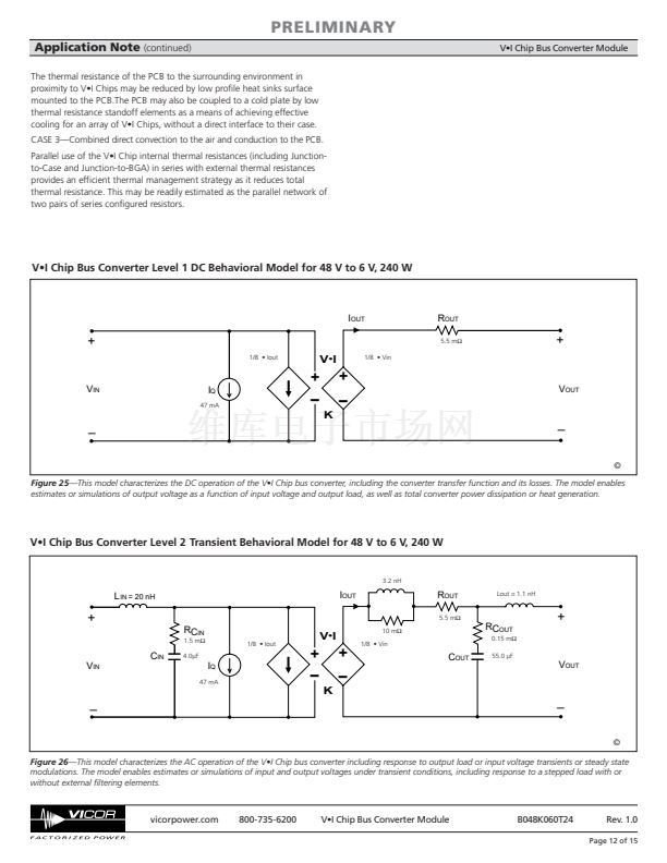
CASE 2鈥擟onduction to the PCB
The low thermal resistance Junction-to-BGA, R胃
JB
, allows use of the PCB
to exchange heat from the V鈥 Chip, including convection from the PCB
to the ambient or conduction to a cold plate.
For example, with a V鈥 Chip surface mounted on a 2" x 2" area of a
multi-layer PCB, with an aggregate 8 oz of effective copper weight, the
total Junction-to-Ambient thermal resistance, R胃
JA
, is 6.5擄C/W in 300
LFM air flow (see Thermal section, Page 6). Given a maximum junction
temperature of 125擄C and 13 W dissipation at 240 W of output power,
a temperature rise of 85擄C allows the V鈥 Chip to operate at rated
output power at up to 40擄C ambient temperature.
V鈥 Chip Bus Converter Module
240
Output Power
0
-40
-20
0
20
40
60
80
100
120
140
Operating Junction Temperature
Figure 23鈥?/div>
Thermal derating curve
BCM with 0.25'' optional Pin Fins
10
9
8
Tja
7
6
5
4
3
0
100
200
300
400
500
600
胃
JC
=
1.1擄C/W
Airflow (LFM)
胃
JB
=
2.1擄C/W
Figure 22鈥擳hermal
resistance
Figure 24鈥擩unction-to-ambient
thermal resistance of BCM with 0.25"
Pin Fins (Pin Fins available as a separate item.)
vicorpower.com
800-735-6200
V鈥 Chip Bus Converter Module
B048K060T24
Rev. 1.0
Page 11 of 15


 1
1
 2
2
 3
3
 4
4
 5
5
 6
6
 7
7
 8
8
 9
9
 10
10
 11
11
 12
12
 13
13
 14
14
 15
15
