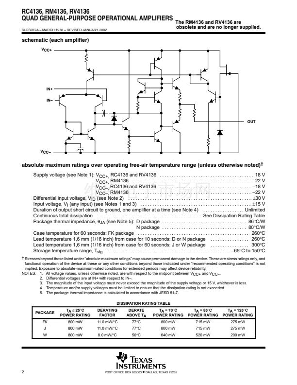
absolute maximum ratings over operating free-air temperature range (unless otherwise noted)
鈥?/div>
Supply voltage (see Note 1): V
CC+,
RC4136 and RV4136 . . . . . . . . . . . . . . . . . . . . . . . . . . . . . . . . . . . . . . . 18 V
V
CC+,
RM4136 . . . . . . . . . . . . . . . . . . . . . . . . . . . . . . . . . . . . . . . . . . . . . . . . . . 22 V
V
CC鈥?
RC4136 and RV4136 . . . . . . . . . . . . . . . . . . . . . . . . . . . . . . . . . . . . . . 鈥?8 V
V
CC鈥?
RM4136 . . . . . . . . . . . . . . . . . . . . . . . . . . . . . . . . . . . . . . . . . . . . . . . . . 鈥?2 V
Differential input voltage, V
ID
(see Note 2) . . . . . . . . . . . . . . . . . . . . . . . . . . . . . . . . . . . . . . . . . . . . . . . . . . .
鹵30
V
Input voltage, V
I
(any input) (see Notes 1 and 3) . . . . . . . . . . . . . . . . . . . . . . . . . . . . . . . . . . . . . . . . . . . . . .
鹵15
V
Duration of output short circuit to ground, one amplifier at a time (see Note 4) . . . . . . . . . . . . . . . . . Unlimited
Continuous total dissipation . . . . . . . . . . . . . . . . . . . . . . . . . . . . . . . . . . . . . . . . . . . See Dissipation Rating Table
Package thermal impedance,
胃
JA
(see Note 5): D package . . . . . . . . . . . . . . . . . . . . . . . . . . . . . . . . . . . 86擄C/W
N package . . . . . . . . . . . . . . . . . . . . . . . . . . . . . . . . . . . 80擄C/W
Case temperature for 60 seconds: FK package . . . . . . . . . . . . . . . . . . . . . . . . . . . . . . . . . . . . . . . . . . . . . . 260擄C
Lead temperature 1,6 mm (1/16 inch) from case for 10 seconds: D or N package . . . . . . . . . . . . . . . . 260擄C
Lead temperature 1,6 mm (1/16 inch) from case for 60 seconds: J or W package . . . . . . . . . . . . . . . . 300擄C
Storage temperature range, T
stg
. . . . . . . . . . . . . . . . . . . . . . . . . . . . . . . . . . . . . . . . . . . . . . . . . . . 鈥?5擄C to 150擄C
鈥?Stresses beyond those listed under 鈥渁bsolute maximum ratings鈥?may cause permanent damage to the device. These are stress ratings only, and
functional operation of the device at these or any other conditions beyond those indicated under 鈥渞ecommended operating conditions鈥?is not
implied. Exposure to absolute-maximum-rated conditions for extended periods may affect device reliability.
NOTES: 1. All voltage values, unless otherwise noted, are with respect to the midpoint between VCC+ and VCC鈥?
2. Differential voltages are at IN+ with respect to IN鈥?
3. The magnitude of the input voltage must never exceed the magnitude of the supply voltage or 15 V, whichever is less.
4. Temperature and/or supply voltages must be limited to ensure that the dissipation rating is not exceeded.
5. The package thermal impedance is calculated in accordance with JESD 51-7.
DISSIPATION RATING TABLE
PACKAGE
FK
J
W
TA
鈮?/div>
25擄C
POWER RATING
800 mW
800 mW
800 mW
DERATING
FACTOR
11.0 mW/擄C
11.0 mW/擄C
8.0 mW/擄C
DERATE
ABOVE TA
77擄C
77擄C
50擄C
TA = 70擄C
POWER RATING
800 mW
800 mW
640 mW
TA = 85擄C
POWER RATING
715 mW
715 mW
520 mW
TA = 125擄C
POWER RATING
275 mW
275 mW
200 mW
2
POST OFFICE BOX 655303
鈥?/div>
DALLAS, TEXAS 75265


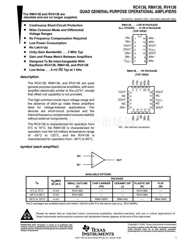 1
1
 2
2
 3
3
 4
4
 5
5
