Pin
Name
Description
The interval between the falling edge of an ON pulse to the first RF amplifier and the rising edge of the next ON
pulse to the first RF amplifier t
PRI
is set by a resistor R
PR
between this pin and ground. The interval t
PRI
can be ad-
justed between 0.1 and 5 碌s with a resistor in the range of 51 K to 2000 K. The value of R
PR
is given by:
R
PR
= 404* t
PRI
+ 10.5, where t
PRI
is in 碌s, and R
PR
is in kilohms
14
PRATE
A 鹵5% resistor value is recommended. When the PWIDTH pin is connected to Vcc through a 1 M resistor, the RF
amplifiers operate at a nominal 50%-50% duty cycle, facilitating high data rate operation. In this case, the period
t
PRC
from start-to-start of ON pulses to the first RF amplifier is controlled by the PRATE resistor over a range of 0.1
to 1.1 碌s using a resistor of 11 K to 220 K. In this case the value of R
PR
is given by:
R
PR
= 198* t
PRC
- 8.51, where t
PRC
is in 碌s and R
PR
is in kilohms
A 鹵5% resistor value should also be used in this case. Please refer to the
ASH Transceiver Designer鈥檚 Guide
for
additional amplifier duty cycle information. It is important to keep the total capacitance between ground, Vcc and
this pin to less than 5 pF to maintain stability.
The PWIDTH pin sets the width of the ON pulse to the first RF amplifier t
PW1
with a resistor R
PW
to ground (the ON
pulse width to the second RF amplifier t
PW2
is set at 1.1 times the pulse width to the first RF amplifier). The ON
pulse width t
PW1
can be adjusted between 0.55 and 1 碌s with a resistor value in the range of 200 K to 390 K. The
value of R
PW
is given by:
R
PW
= 404* t
PW1
- 18.6, where t
PW1
is in 碌s and R
PW
is in kilohms
A 鹵5% resistor value is recommended. When this pin is connected to Vcc through a 1 M resistor, the RF amplifi-
ers operate at a nominal 50%-50% duty cycle, facilitating high data rate operation. In this case, the RF amplifier
ON times are controlled by the PRATE resistor as described above. It is important to keep the total capacitance
between ground, Vcc and this node to less than 5 pF to maintain stability. When using the high data rate operation
with the sleep mode, connect the 1 M resistor between this pin and CNTRL1 (Pin 17), so this pin is low in the
sleep mode.
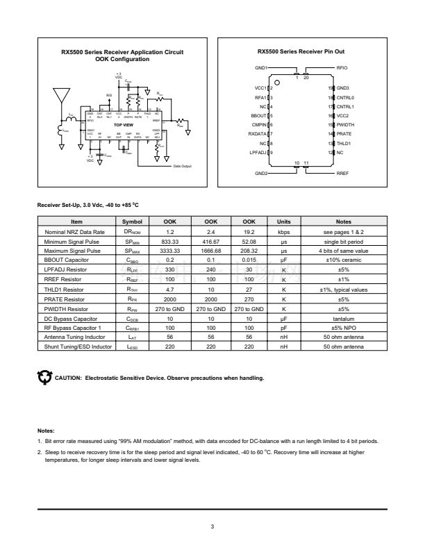
VCC2 is the positive supply voltage pin for the receiver RF section. This pin must be bypassed with an RF capaci-
tor, which may be shared with VCC1. VCC2 must also be bypassed with a 1 to 10 碌F tantalum or electrolytic ca-
pacitor.
CNTRL1 and CNTRL0 select the receiver modes. CNTRL1 and CNTRL0 both high place the unit in the receive
mode. CNTRL1 and CNTRL0 both low place the unit in the power-down (sleep) mode. CNTRL1 is a
high-impedance input (CMOS compatible). An input voltage of 0 to 300 mV is interpreted as a logic low. An input
voltage of Vcc - 300 mV or greater is interpreted as a logic high. An input voltage greater than Vcc + 200 mV
should not be applied to this pin. A logic high requires a maximum source current of 40 碌A(chǔ). Sleep mode requires a
maximum sink current of 1 碌A(chǔ). This pin must be held at a logic level; it cannot be left unconnected. At turn on, the
voltage on this pin and CNTRL0 should rise with Vcc until Vcc reaches 2.7 Vdc (receive mode). Thereafter, the
sleep mode can be selected.
CNTRL0 is used with CNTRL1 to control the receiver modes. CNTRL0 is a high-impedance input (CMOS compat-
ible). An input voltage of 0 to 300 mV is interpreted as a logic low. An input voltage of Vcc - 300 mV or greater is
interpreted as a logic high. An input voltage greater than Vcc + 200 mV should not be applied to this pin. A logic
high requires a maximum source current of 40 碌A(chǔ). Sleep mode requires a maximum sink current of 1 碌A(chǔ). This pin
must be held at a logic level; it cannot be left unconnected. At turn on, the voltage on this pin and CNTRL1 should
rise with Vcc until Vcc reaches 2.7 Vdc (receive mode). Thereafter, the sleep mode can be selected.
GND3 is an IC ground pin. It should be connected to GND1 by a short, low inductance trace.
RFIO is the receiver RF input pin. This pin is connected directly to the SAW filter transducer. Antennas presenting
an impedance in the range of 35 to 72 ohms resistive can be satisfactorily matched to this pin with a series match-
ing coil and a shunt matching/ESD protection coil. Other antenna impedances can be matched using two or three
components. For some impedances, two inductors and a capacitor will be required. A DC path from RFIO to
ground is required for ESD protection.
15
PWIDTH
16
VCC2
17
CNTRL1
18
CNTRL0
19
GND3
20
RFIO
9


 1
1
 2
2
 3
3
 4
4
 5
5
 6
6
 7
7
 8
8
 9
9
 10
10
