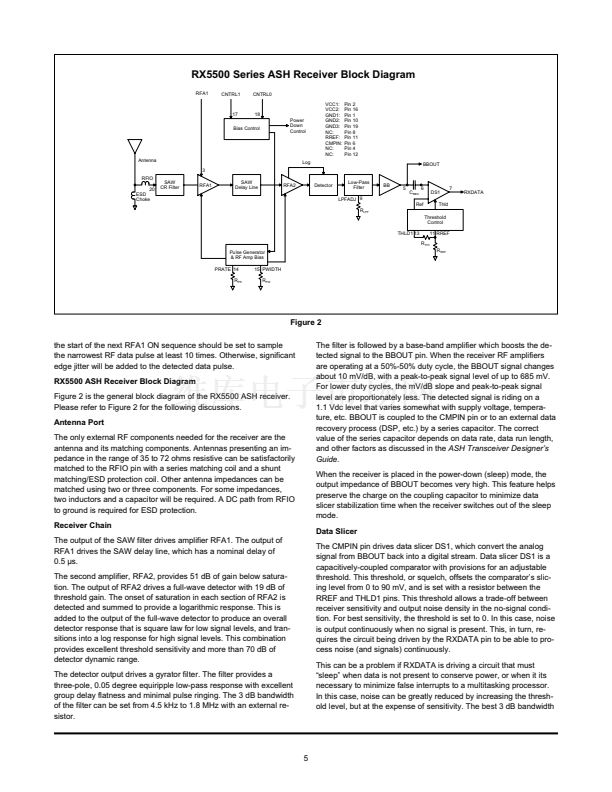
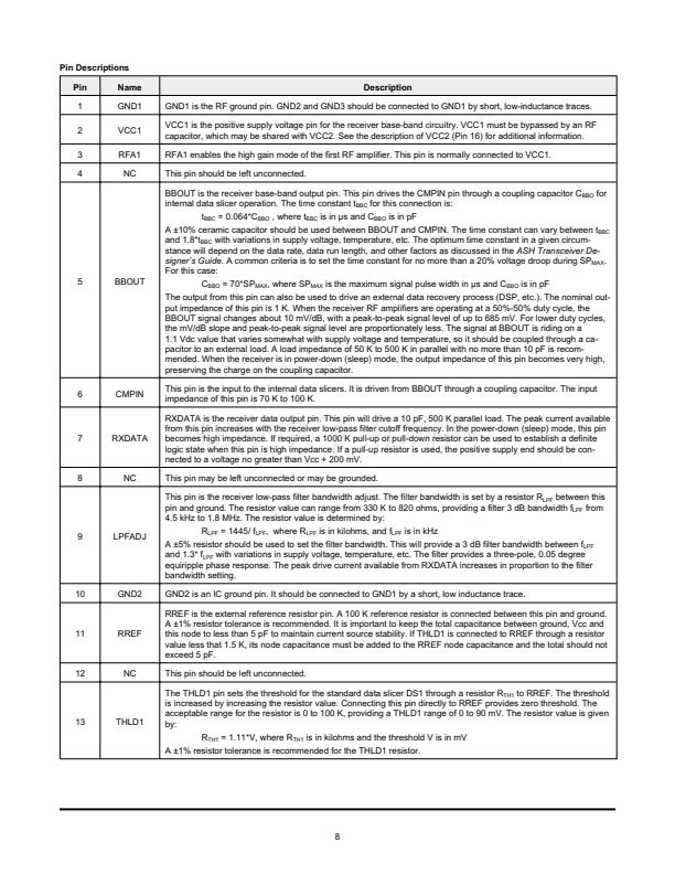
Pin Descriptions
Pin
1
2
3
4
Name
GND1
VCC1
RFA1
NC
Description
GND1 is the RF ground pin. GND2 and GND3 should be connected to GND1 by short, low-inductance traces.
VCC1 is the positive supply voltage pin for the receiver base-band circuitry. VCC1 must be bypassed by an RF
capacitor, which may be shared with VCC2. See the description of VCC2 (Pin 16) for additional information.
RFA1 enables the high gain mode of the first RF amplifier. This pin is normally connected to VCC1.
This pin should be left unconnected.
BBOUT is the receiver base-band output pin. This pin drives the CMPIN pin through a coupling capacitor C
BBO
for
internal data slicer operation. The time constant t
BBC
for this connection is:
t
BBC
= 0.064*C
BBO
, where t
BBC
is in 碌s and C
BBO
is in pF
A 鹵10% ceramic capacitor should be used between BBOUT and CMPIN. The time constant can vary between t
BBC
and 1.8*t
BBC
with variations in supply voltage, temperature, etc. The optimum time constant in a given circum-
stance will depend on the data rate, data run length, and other factors as discussed in the
ASH Transceiver De-
signer鈥檚 Guide.
A common criteria is to set the time constant for no more than a 20% voltage droop during SP
MAX
.
For this case:
C
BBO
= 70*SP
MAX
, where SP
MAX
is the maximum signal pulse width in 碌s and C
BBO
is in pF
The output from this pin can also be used to drive an external data recovery process (DSP, etc.). The nominal out-
put impedance of this pin is 1 K. When the receiver RF amplifiers are operating at a 50%-50% duty cycle, the
BBOUT signal changes about 10 mV/dB, with a peak-to-peak signal level of up to 685 mV. For lower duty cycles,
the mV/dB slope and peak-to-peak signal level are proportionately less. The signal at BBOUT is riding on a
1.1 Vdc value that varies somewhat with supply voltage and temperature, so it should be coupled through a ca-
pacitor to an external load. A load impedance of 50 K to 500 K in parallel with no more than 10 pF is recom-
mended. When the receiver is in power-down (sleep) mode, the output impedance of this pin becomes very high,
preserving the charge on the coupling capacitor.
6
CMPIN
This pin is the input to the internal data slicers. It is driven from BBOUT through a coupling capacitor. The input
impedance of this pin is 70 K to 100 K.
RXDATA is the receiver data output pin. This pin will drive a 10 pF, 500 K parallel load. The peak current available
from this pin increases with the receiver low-pass filter cutoff frequency. In the power-down (sleep) mode, this pin
becomes high impedance. If required, a 1000 K pull-up or pull-down resistor can be used to establish a definite
logic state when this pin is high impedance. If a pull-up resistor is used, the positive supply end should be con-
nected to a voltage no greater than Vcc + 200 mV.
This pin may be left unconnected or may be grounded.
This pin is the receiver low-pass filter bandwidth adjust. The filter bandwidth is set by a resistor R
LPF
between this
pin and ground. The resistor value can range from 330 K to 820 ohms, providing a filter 3 dB bandwidth f
LPF
from
4.5 kHz to 1.8 MHz. The resistor value is determined by:
R
LPF
= 1445/ f
LPF
, where R
LPF
is in kilohms, and f
LPF
is in kHz
A 鹵5% resistor should be used to set the filter bandwidth. This will provide a 3 dB filter bandwidth between f
LPF
and 1.3* f
LPF
with variations in supply voltage, temperature, etc. The filter provides a three-pole, 0.05 degree
equiripple phase response. The peak drive current available from RXDATA increases in proportion to the filter
bandwidth setting.
GND2 is an IC ground pin. It should be connected to GND1 by a short, low inductance trace.
RREF is the external reference resistor pin. A 100 K reference resistor is connected between this pin and ground.
A 鹵1% resistor tolerance is recommended. It is important to keep the total capacitance between ground, Vcc and
this node to less than 5 pF to maintain current source stability. If THLD1 is connected to RREF through a resistor
value less that 1.5 K, its node capacitance must be added to the RREF node capacitance and the total should not
exceed 5 pF.
This pin should be left unconnected.
The THLD1 pin sets the threshold for the standard data slicer DS1 through a resistor R
TH1
to RREF. The threshold
is increased by increasing the resistor value. Connecting this pin directly to RREF provides zero threshold. The
acceptable range for the resistor is 0 to 100 K, providing a THLD1 range of 0 to 90 mV. The resistor value is given
by:
R
TH1
= 1.11*V, where R
TH1
is in kilohms and the threshold V is in mV
A 鹵1% resistor tolerance is recommended for the THLD1 resistor.
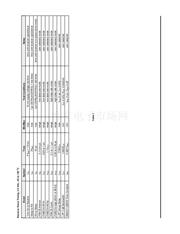
5
BBOUT
7
RXDATA
8
NC
9
LPFADJ
10
GND2
11
RREF
12
NC
13
THLD1
8


 1
1
 2
2
 3
3
 4
4
 5
5
 6
6
 7
7
 8
8
 9
9
 10
10
