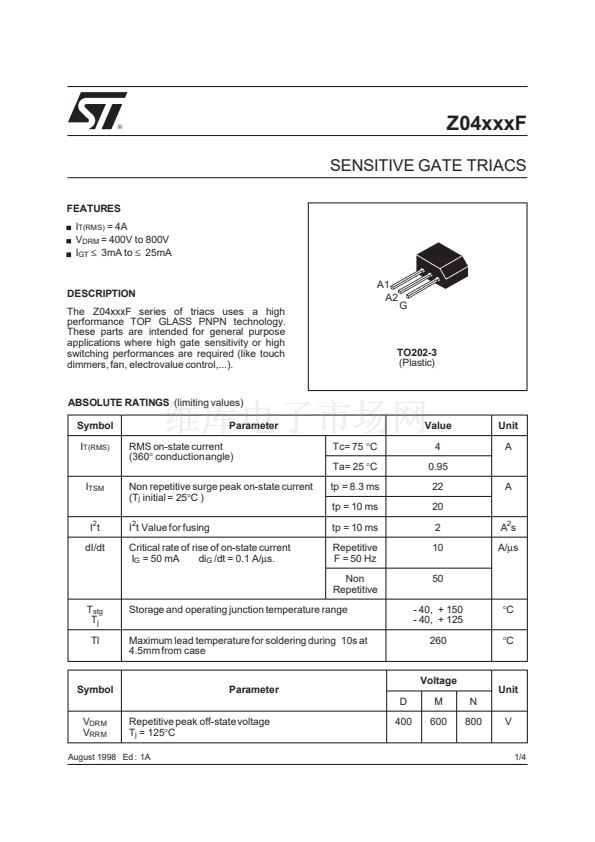
Z04xxxF
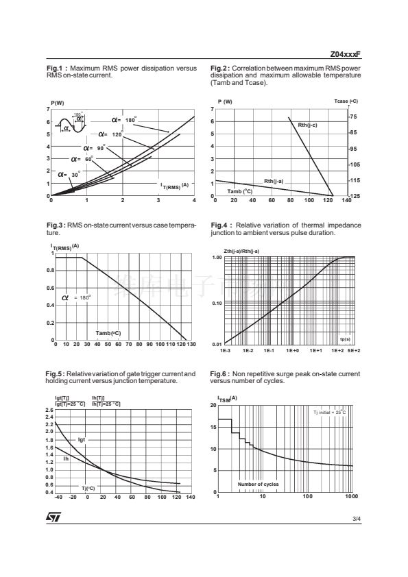
Fig.1 :
Maximum RMS power dissipation versus
RMS on-state current.
Fig.2 :
Correlation between maximum RMS power
dissipation and maximum allowable temperature
(Tamb and Tcase).
P (W)
180
O
P(W)
Tcase (
o
C)
7
6
5
4
3
2
1
0
0
7
= 180
= 120
= 90
o
o
o
6
5
4
3
-75
Rth(j-c)
-85
-95
-105
= 60
= 30
o
o
2
I
T(RMS)
(A)
1
4
0
0
Tamb ( C)
o
Rth(j-a)
-115
-125
140
1
2
3
20
40
60
80
100
120
Fig.3 :
RMS on-state current versus case tempera-
ture.
I T(RMS) (A)
Fig.4 :
Relative variation of thermal impedance
junction to ambient versus pulse duration.
Zth(j-a)/Rth(j-a)
1.00
1
0.8
0.6
= 180
o
0.4
0.2
0.10
Tamb(
o
C)
0
0
tp( s)
10 20 30 40 50 60 70 80 90 100 110 120 130
0.01
1E-3
1E-2
1E-1
1 E +0
1 E +1
1E +2 5 E +2
Fig.5 :
Relativevariation of gate trigger current and
holding current versus junction temperature.
Igt[Tj]
o
Igt[Tj=25 C]
Ih[Tj]
o
Ih[Tj=25 C]
Fig.6 :
Non repetitive surge peak on-state current
versus number of cycles.
ITSM(A)
2.6
2.4
2.2
2.0
1.8
1.6
1.4
1.2
1.0
0.8
0.6
0.4
Igt
20
Tj initial = 25 C
o
15
10
Ih
5
Tj(
o
C)
Number of cycles
-40
-20
0
20
40
60
80
100
120 140
0
1
10
100
1000
3/4


 1
1
 2
2
 3
3
 4
4
