PLL102-03
Low Skew Output Buffer
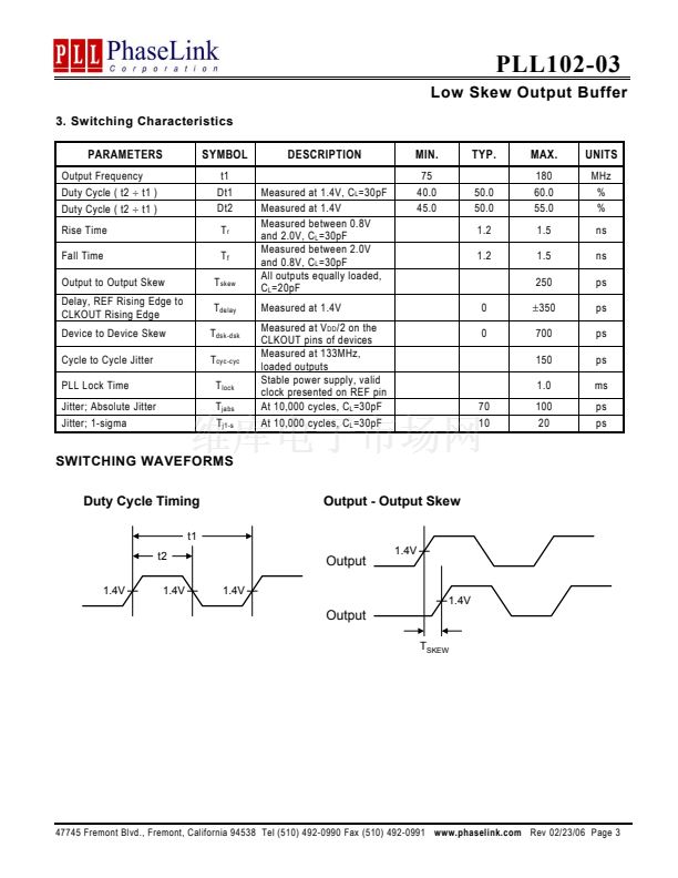
3. Switching Characteristics
PARAMETERS
Output Frequency
Duty Cycle ( t2
梅
t1 )
Duty Cycle ( t2
梅
t1 )
Rise Time
Fall Time
Output to Output Skew
Delay, REF Rising Edge to
CLKOUT Rising Edge
Device to Device Skew
Cycle to Cycle Jitter
PLL Lock Time
Jitter; Absolute Jitter
Jitter; 1-sigma
SYMBOL
t1
Dt1
Dt2
T
r
T
f
T
skew
T
delay
T
dsk-dsk
T
cyc-cyc
T
lock
T
jabs
T
j1-s
DESCRIPTION
Measured at 1.4V, C
L
=30pF
Measured at 1.4V
Measured between 0.8V
and 2.0V, C
L
=30pF
Measured between 2.0V
and 0.8V, C
L
=30pF
All outputs equally loaded,
C
L
=20pF
Measured at 1.4V
Measured at V
DD
/2 on the
CLKOUT pins of devices
Measured at 133MHz,
loaded outputs
Stable power supply, valid
clock presented on REF pin
At 10,000 cycles, C
L
=30pF
At 10,000 cycles, C
L
=30pF
MIN.
75
40.0
45.0
TYP.
50.0
50.0
1.2
1.2
MAX.
180
60.0
55.0
1.5
1.5
250
UNITS
MHz
%
%
ns
ns
ps
ps
ps
ps
ms
ps
ps
0
0
鹵350
700
150
1.0
70
10
100
20
SWITCHING WAVEFORMS
Duty Cycle Timing
t1
t2
1.4V
1.4V
1.4V
Output - Output Skew
Output
1.4V
1.4V
Output
T
SKEW
47745 Fremont Blvd., Fremont, California 94538 Tel (510) 492-0990 Fax (510) 492-0991
www.phaselink.com
Rev 02/23/06 Page 3


 1
1
 2
2
 3
3
 4
4
 5
5
 6
6
