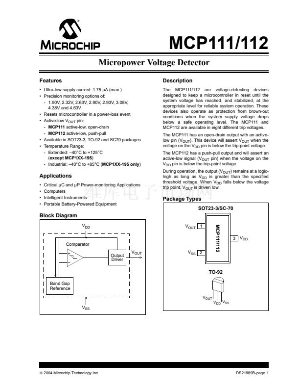
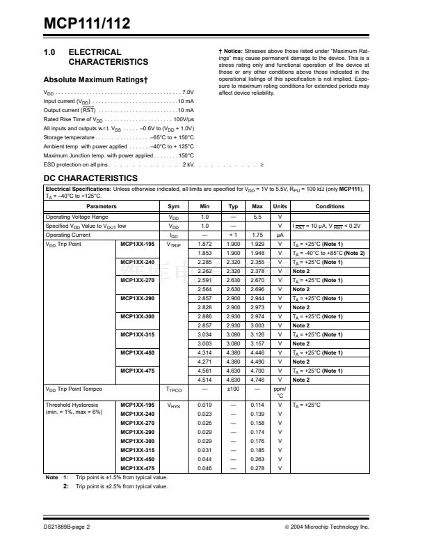
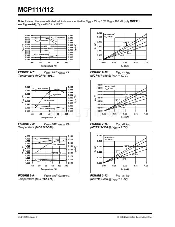
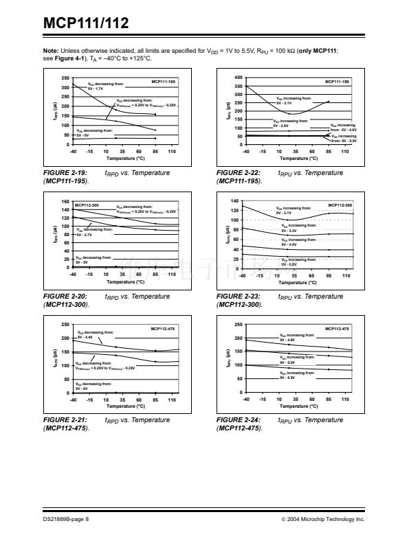
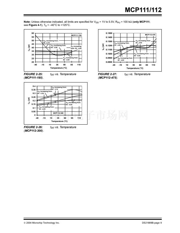
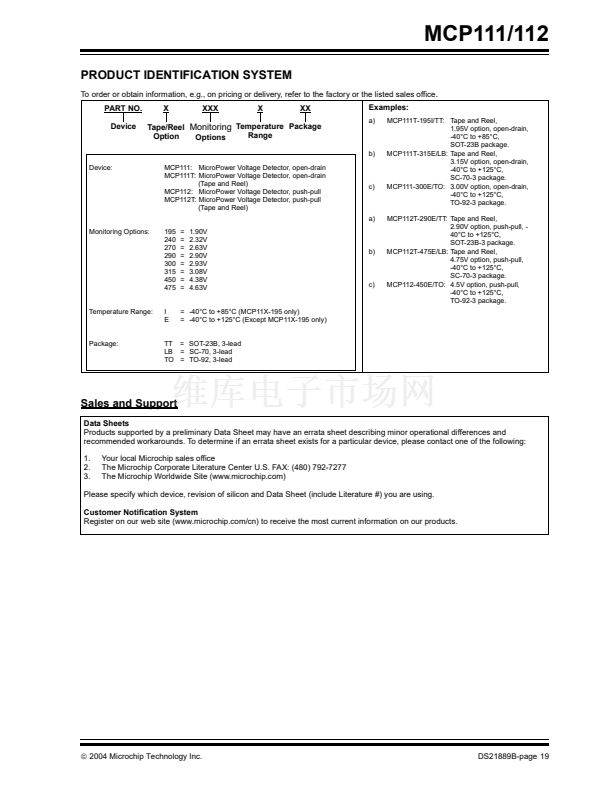
MCP111/112
4.0
APPLICATION INFORMATION
4.1
V
TRIP
Operation
For many of today鈥檚 microcontroller applications, care
must be taken to prevent low-power conditions that can
cause many different system problems. The most
common causes are brown-out conditions, where the
system supply drops below the operating level momen-
tarily. The second most common cause is when a slowly
decaying power supply causes the microcontroller to
begin executing instructions without sufficient voltage to
sustain SRAM, thus producing indeterminate results.
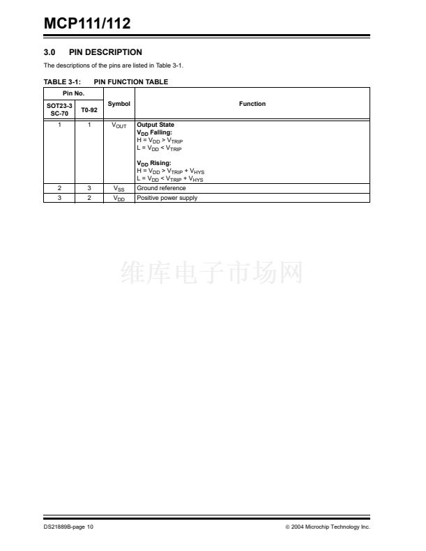
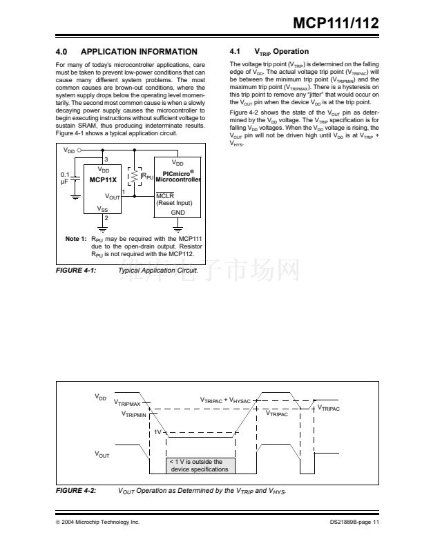
Figure 4-1 shows a typical application circuit.
V
DD
3
0.1
碌F
V
DD
V
DD
R
PU
1
PICmicro
廬
Microcontroller
MCLR
(Reset Input)
GND
The voltage trip point (V
TRIP
) is determined on the falling
edge of V
DD
. The actual voltage trip point (V
TRIPAC
) will
be between the minimum trip point (V
TRIPMIN
) and the
maximum trip point (V
TRIPMAX
). There is a hysteresis on
this trip point to remove any 鈥渏itter鈥?that would occur on
the V
OUT
pin when the device V
DD
is at the trip point.
Figure 4-2 shows the state of the V
OUT
pin as deter-
mined by the V
DD
voltage. The V
TRIP
specification is for
falling V
DD
voltages. When the V
DD
voltage is rising, the
V
OUT
pin will not be driven high until V
DD
is at V
TRIP
+
V
HYS
.
MCP11X
V
OUT
V
SS
2
Note 1:
R
PU
may be required with the MCP111
due to the open-drain output. Resistor
R
PU
is not required with the MCP112.
FIGURE 4-1:
Typical Application Circuit.
V
DD
V
TRIPMAX
V
TRIPMIN
1V
V
TRIPAC
+ V
HYSAC
V
TRIPAC
V
TRIPAC
V
OUT
< 1 V is outside the
device specifications
FIGURE 4-2:
V
OUT
Operation as Determined by the V
TRIP
and V
HYS
.
錚?/div>
2004 Microchip Technology Inc.
DS21889B-page 11


 1
1
 2
2
 3
3
 4
4
 5
5
 6
6
 7
7
 8
8
 9
9
 10
10
 11
11
 12
12
 13
13
 14
14
 15
15
 16
16
 17
17
 18
18
 19
19
 20
20
 21
21
 22
22
