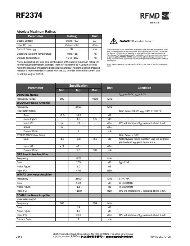
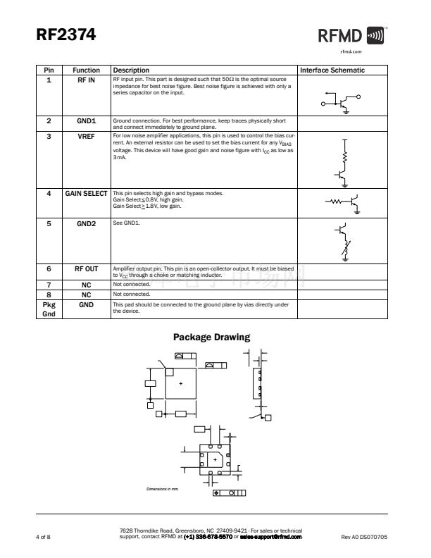
RF2374
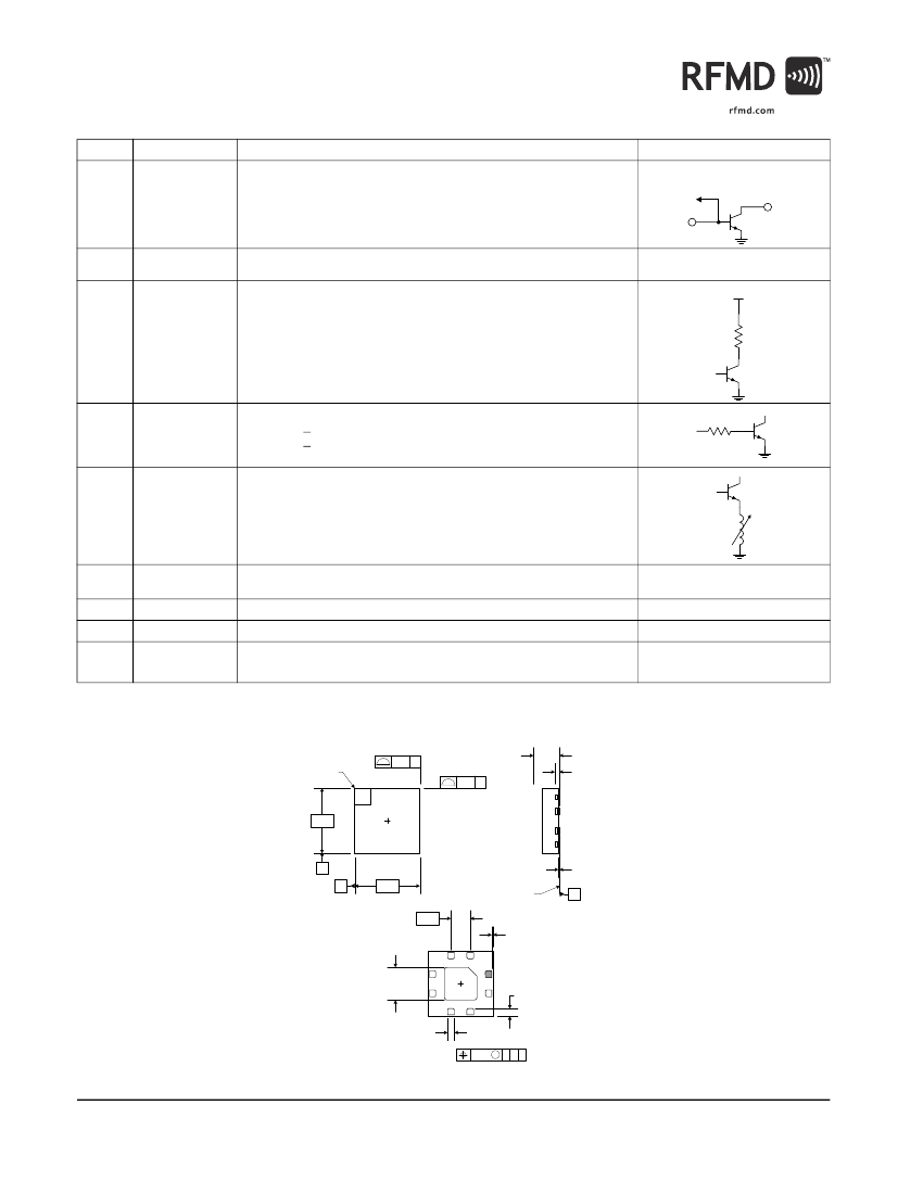
Pin
1
Function
RF IN
Description
RF input pin. This part is designed such that 50惟 is the optimal source
impedance for best noise figure. Best noise figure is achieved with only a
series capacitor on the input.
RF IN
Interface Schematic
To Bias
Circuit
RF OUT
2
3
GND1
VREF
Ground connection. For best performance, keep traces physically short
and connect immediately to ground plane.
For low noise amplifier applications, this pin is used to control the bias cur-
rent. An external resistor can be used to set the bias current for any V
BIAS
voltage. This device will have good gain and noise figure with I
CC
as low as
3mA.
VREF
4
GAIN SELECT
This pin selects high gain and bypass modes.
Gain Select<0.8V, high gain.
Gain Select>1.8V, low gain.
See GND1.
5
GND2
6
7
8
Pkg
Gnd
RF OUT
NC
NC
GND
Amplifier output pin. This pin is an open-collector output. It must be biased
to V
CC
through a choke or matching inductor.
Not connected.
Not connected.
This pad should be connected to the ground plane by vias directly under
the device.
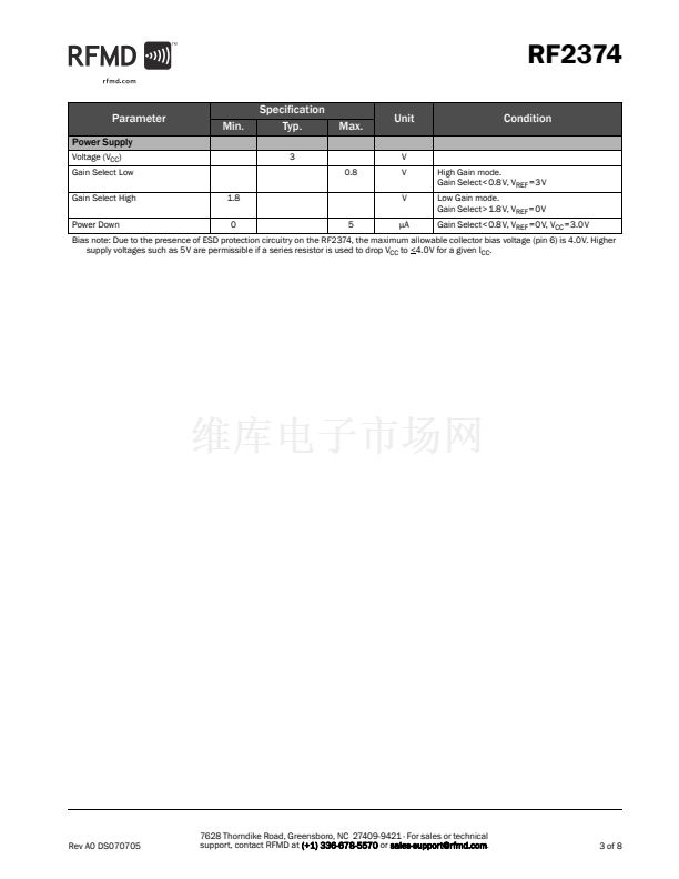
Package Drawing
INDEX
AREA
2 PLCS
0.10 C
0.10 C
2 PLCS
0.63
0.53
0.152
REF
2.20
B
A
2.20
0.65
0.05
0.00
SEATING
PLANE
C
0.10
MAX
1.20
TYP
1.00
0.28
0.18
0.31
0.21
Dimensions in mm.
Shaded lead is pin 1.
0.10 M C A B
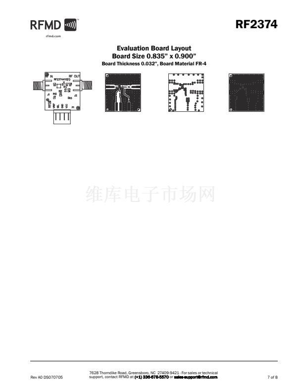
4 of 8
7628 Thorndike Road, Greensboro, NC 27409-9421 路 For sales or technical
support, contact RFMD at (+1) 336-678-5570 or sales-support@rfmd.com.
Rev A0 DS070705


 1
1
 2
2
 3
3
 4
4
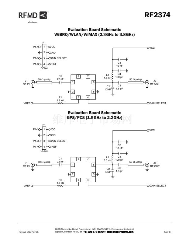 5
5
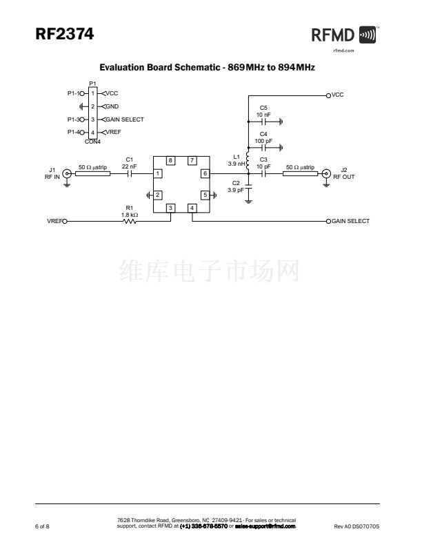 6
6
 7
7
 8
8
