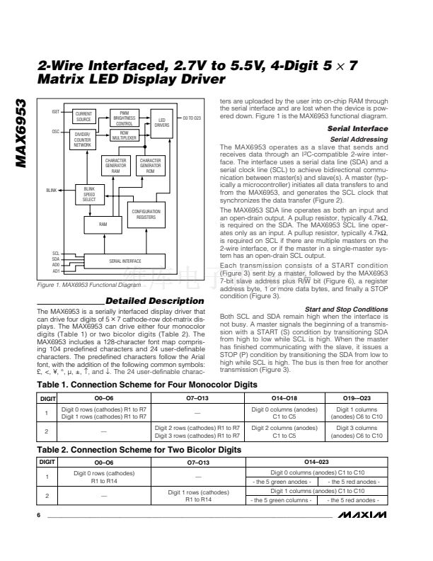
鉁?/div>
7
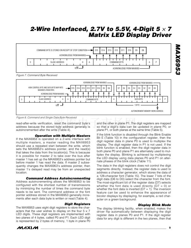
ACKNOWLEDGE FROM MAX6953
D1
D0
A
P
R/W
AUTOINCREMENT MEMORY WORD ADDRESS
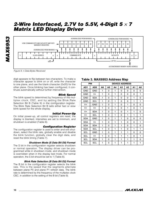
Figure 9. n Data Bytes Received
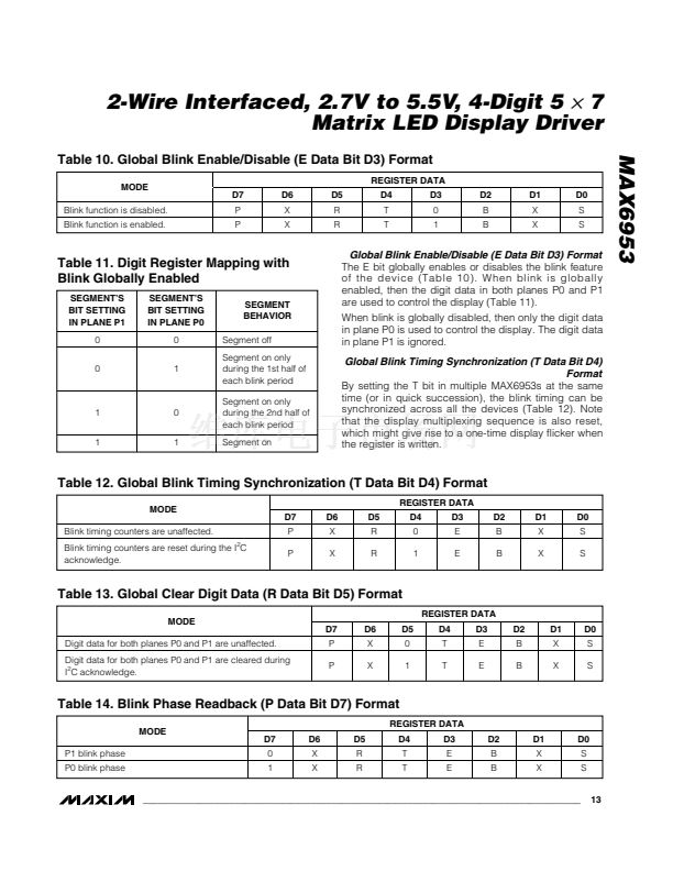
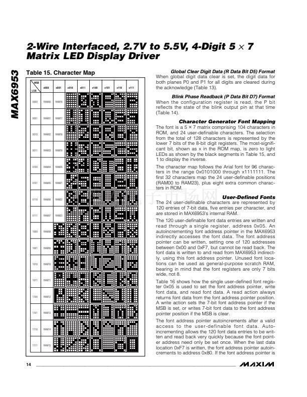
digit appears to flip between two characters. To make a
character appear to blink on or off, write the character
to one plane, and use the blank character (0x20) for the
other plane. Once blinking has been configured, it con-
tinues automatically without further intervention.
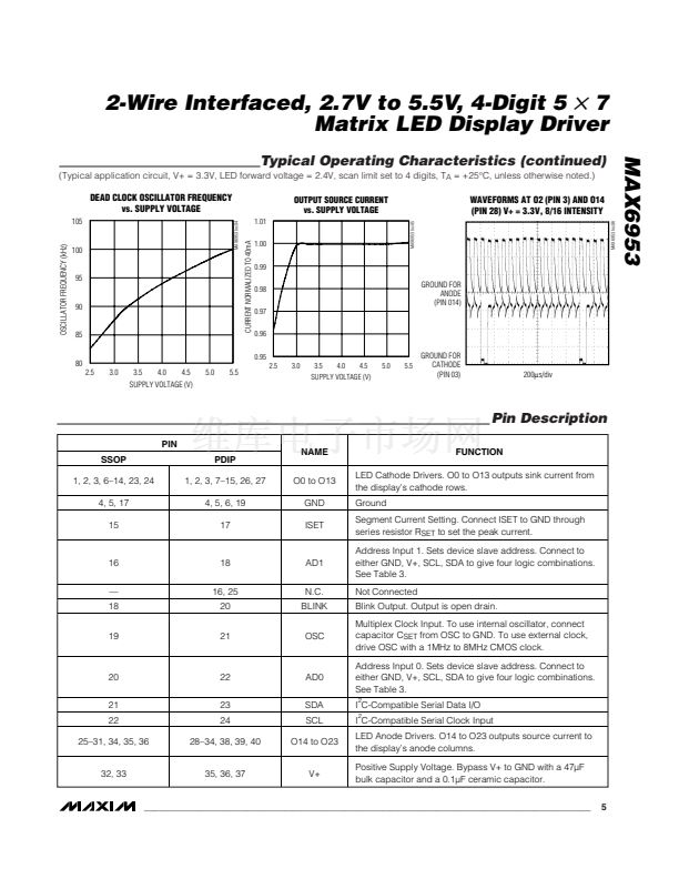
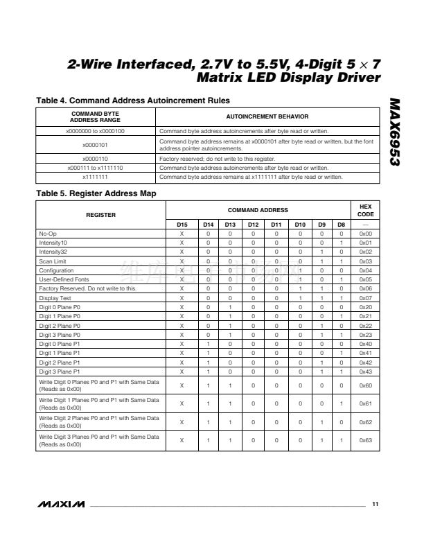
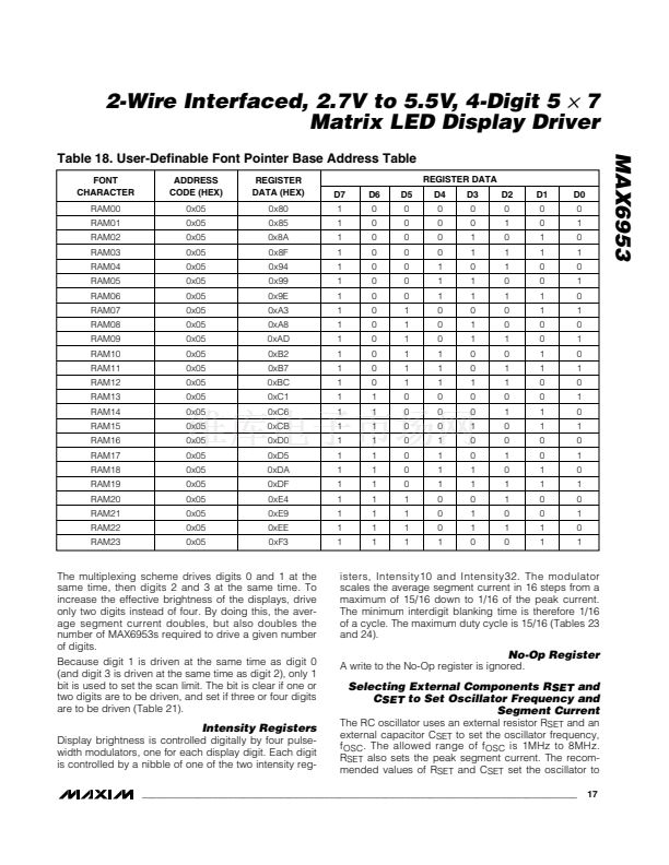
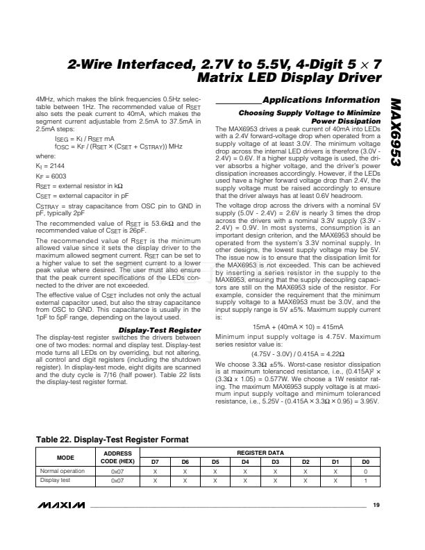
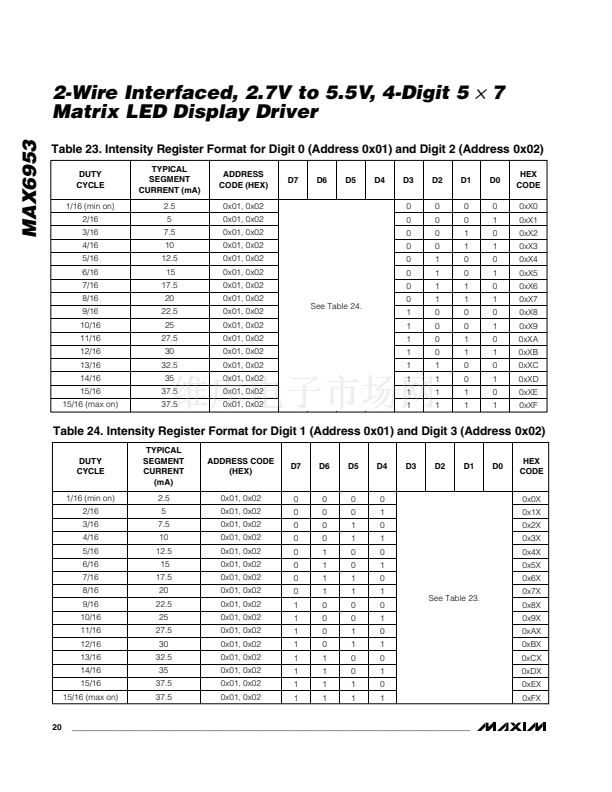
Table 3. MAX6953 Address Map
PIN
AD1
GND
GND
GND
GND
V+
V+
V+
V+
SDA
SDA
SDA
SDA
SCL
SCL
SCL
SCL
AD0
GND
V+
SDA
SCL
GND
V+
SDA
SCL
GND
V+
SDA
SCL
GND
V+
SDA
SCL
A6
1
1
1
1
1
1
1
1
1
1
1
1
1
1
1
1
A5
0
0
0
0
0
0
0
0
0
0
0
0
0
0
0
0
DEVICE ADDRESS
A4
1
1
1
1
1
1
1
1
1
1
1
1
1
1
1
1
A3
0
0
0
0
0
0
0
0
1
1
1
1
1
1
1
1
A2
0
0
0
0
1
1
1
1
0
0
0
0
1
1
1
1
A1
0
0
1
1
0
0
1
1
0
0
1
1
0
0
1
1
A0
0
1
0
1
0
1
0
1
0
1
0
1
0
1
0
1
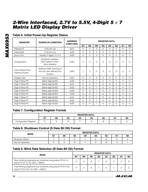
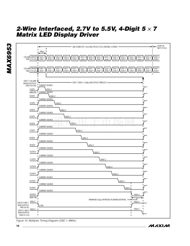
Blink Speed
The blink speed is determined by frequency of the mul-
tiplex clock, OSC, and by setting the Blink Rate
Selection Bit B (Table 9) in the configuration register.
The Blink Rate Selection Bit B sets either fast or slow
blink speed for the whole display.
Initial Power-Up
On initial power-up, all control registers are reset, the
display is blanked, intensities are set to minimum, and
shutdown is enabled (Table 6).
Configuration Register
The configuration register is used to enter and exit shut-
down, select the blink rate, globally enable and disable
the blink function, globally clear the digit data, and
reset the blink timing (Table 7).
Shutdown Mode (S Data Bit D0) Format
The S bit in the configuration register selects shutdown
or normal operation. The display driver can be pro-
grammed while in shutdown mode, and shutdown mode
is overridden when in the display test mode. For normal
operation, the S bit should be set to 1 (Table 8).
Blink Rate Selection (B Data Bit D2) Format
The B bit in the configuration register selects the blink
rate. This is the speed that the segments alternate
between plane P0 and plane P1 refresh data. The blink
rate is determined by the frequency of the multiplex clock
OSC, in addition to the setting of the B bit (Table 9).
10
______________________________________________________________________________________


 1
1
 2
2
 3
3
 4
4
 5
5
 6
6
 7
7
 8
8
 9
9
 10
10
 11
11
 12
12
 13
13
 14
14
 15
15
 16
16
 17
17
 18
18
 19
19
 20
20
 21
21
 22
22
 23
23
