鈮?/div>
2.3V and V
IN
鈮?(V
R
+ 2.5%)
+
V
DROPOUT.
V
R
is the nominal regulator output voltage for the fixed cases. V
R
= 1.2V, 1.8V, etc. V
R
is the desired set
point output voltage for the adjustable cases. V
R
= V
ADJ *
((R
1
/R
2
)+1). Figure 4-1.
TCV
OUT
= (V
OUT-HIGH
鈥?V
OUT-LOW
) *10
6
/ (V
R
*
螖Temperature).
V
OUT-HIGH
is the highest voltage measured
over the temperature range. V
OUT-LOW
is the lowest voltage measured over the temperature range.
Load regulation is measured at a constant junction temperature using low duty-cycle pulse testing. Load
regulation is tested over a load range from 1 mA to the maximum specified output current.
Dropout voltage is defined as the input-to-output voltage differential at which the output voltage drops 2%
below its nominal value that was measured with an input voltage of V
IN
= V
R
+ 0.5V.
The maximum allowable power dissipation is a function of ambient temperature, the maximum allowable
junction temperature and the thermal resistance from junction to air. (i.e., T
A
, T
J
,
胃
J
A
). Exceeding the maxi-
mum allowable power dissipation will cause the device operating junction temperature to exceed the maxi-
mum 150擄C rating. Sustained junction temperatures above 125擄C can impact device reliability.
The junction temperature is approximated by soaking the device under test at an ambient temperature
equal to the desired junction temperature. The test time is small enough such that the rise in the junction
temperature over the ambient temperature is not significant.
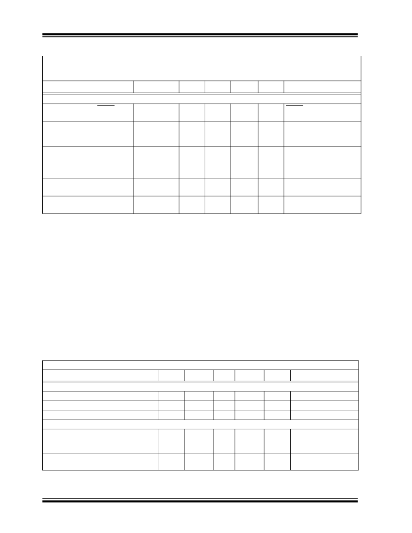
TEMPERATURE SPECIFICATIONS
Electrical Specifications:
Unless otherwise indicated, all limits apply for V
IN
= 2.3V to 6.0V.
Parameters
Temperature Ranges
Operating Junction Temperature Range
Maximum Junction Temperature
Storage Temperature Range
Thermal Package Resistances
Thermal Resistance, 8LD 3 x 3 DFN
胃
JA
鈥?/div>
41
鈥?/div>
擄C/W
4-Layer JC51-7
Standard Board with
vias
4-Layer JC51-7
Standard Board
T
J
T
J
T
A
-40
鈥?/div>
-65
鈥?/div>
鈥?/div>
鈥?/div>
+125
+150
+150
擄C
擄C
擄C
Steady State
Transient
Sym
Min
Typ
Max
Units
Conditions
Thermal Resistance, 8LD SOIC
胃
JA
鈥?/div>
150
鈥?/div>
擄C/W
DS21936B-page 6
漏
2005 Microchip Technology Inc.
MCP1726-ADJE/MF 產(chǎn)品屬性
Microchip
低壓降 (LDO) 調(diào)節(jié)器
6 V
0.8 V to 5 V
0.5 V at 1 A
1 A
0.5 %
1
Adjustable
+ 125 C
SMD/SMT
DFN-8
0.14 mA
+ 2.3 V
0.05 % / V
- 40 C
Tube
0.41 V
120
2.5 %
MCP1726-ADJE/MF相關(guān)型號(hào)PDF文件下載
-
型號(hào)
版本
描述
廠商
下載
-
英文版
Microcontroller Supervisory Circuit with Push-Pull Output
-
英文版
Microcontroller Supervisory Circuit with Push-Pull Output
MICROCHIP ...
-
英文版
Microcontroller Supervisory Circuit with Push-Pull Output
-
英文版
Microcontroller Supervisory Circuit with Push-Pull Output
MICROCHIP ...
-
英文版
Micropower Voltage Supervisors
-
英文版
Micropower Voltage Supervisors
-
英文版
Micropower Voltage Detector
-
英文版
Micropower Voltage Detector
MICROCHIP ...
-
英文版
Micropower Voltage Detector
-
英文版
Micropower Voltage Detector
MICROCHIP ...
-
英文版
Microcontroller Supervisory Circuit with Open Drain Output
-
英文版
Microcontroller Supervisory Circuit with Open Drain Output
MICROCHIP ...
-
英文版
Micropower Voltage Supervisors
-
英文版
Microcontroller Supervisory Circuit with Open Drain Output
-
英文版
Microcontroller Supervisory Circuit with Open Drain Output
MICROCHIP ...
-
英文版
Micropower Voltage Supervisors
-
英文版
Microcontroller Supervisory Circuit with Open Drain Output
-
英文版
Microcontroller Supervisory Circuit with Open Drain Output
MICROCHIP ...
-
英文版
Low Noise, Positive-Regulated Charge Pump
-
英文版
Low Noise, Positive-Regulated Charge Pump
MICROCHIP ...


 1
1
 2
2
 3
3
 4
4
 5
5
 6
6
 7
7
 8
8
 9
9
 10
10
 11
11
 12
12
 13
13
 14
14
 15
15
 16
16
 17
17
 18
18
 19
19
 20
20
 21
21
 22
22
 23
23
 24
24
 25
25
 26
26
 27
27
 28
28
 29
29
 30
30
