MCP1726
5.0
5.1
APPLICATION
CIRCUITS/ISSUES
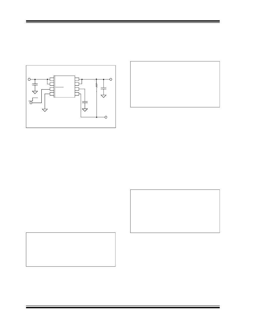
Typical Application
In addition to the LDO pass element power dissipation,
there is power dissipation within the MCP1726 as a
result of quiescent or ground current. The power dissi-
pation as a result of the ground current can be
calculated using the following equation:
The MCP1726 is used for applications that require high
LDO output current and a power good output.
MCP1726-2.5
V
IN
= 3.3V
1 V
IN
C
1
10 碌F
On
Off
2 V
IN
V
OUT
8
V
OUT
7
R
1
10k惟
C
2
10 碌F
V
OUT
= 2.5V @ 1A
EQUATION 5-2:
P
I
(
GND
)
=
V
IN
(
MAX
)
脳
I
VIN
P
I(GND)
= Power dissipation due to the
quiescent current of the LDO
V
IN(MAX)
= Maximum input voltage
I
VIN
= Current flowing in the V
IN
pin with
no LDO output current (LDO
quiescent current)
The total power dissipated within the MCP1726 is the
sum of the power dissipated in the LDO pass device
and the P(I
GND
) term. Because of the CMOS construc-
tion, the typical I
GND
for the MCP1726 is 140 碌A(chǔ).
Operating at a maximum of 3.63V results in a power
dissipation of 0.51 milli-Watts. For most applications,
this is small compared to the LDO pass device power
dissipation and can be neglected.
The maximum continuous operating junction tempera-
ture specified for the MCP1726 is +125
擄
C
.
To estimate
the internal junction temperature of the MCP1726, the
total internal power dissipation is multiplied by the ther-
mal resistance from junction to ambient (R胃
JA
) of the
device. The thermal resistance from junction to ambi-
ent for the 3X3DFN package is estimated at 41
擄
C/W.
3 SHDN C
DELAY
6
4 GND PWRGD 5
C
3
1000 pF
PWRGD
FIGURE 5-1:
5.1.1
Typical Application Circuit.
APPLICATION CONDITIONS
Package Type = 3X3DFN8
Input Voltage Range = 3.3V 鹵 10%
V
IN
maximum = 3.63V
V
IN
minimum = 2.97V
V
OUT
typical = 2.5V
I
OUT
= 1.0A maximum
5.2
5.2.1
Power Calculations
POWER DISSIPATION
EQUATION 5-3:
T
J
(
MAX
)
=
P
TOTAL
脳
R胃
JA
+
T
AMAX
T
J(MAX)
= Maximum continuous junction
temperature
P
TOTAL
= Total device power dissipation
R胃
JA
= Thermal resistance from junction
to ambient
T
AMAX
= Maximum ambient temperature
The internal power dissipation within the MCP1726 is a
function of input voltage, output voltage, output current
and quiescent current. The following equation can be
used to calculate the internal power dissipation for the
LDO.
EQUATION 5-1:
P
LDO
=
(
V
IN
(
MAX
) )
鈥?/div>
V
OUT
(
MIN
)
) 脳
I
OUT
(
MAX
) )
P
LDO
= LDO Pass device internal power
dissipation
V
IN(MAX)
= Maximum input voltage
V
OUT(MIN)
= LDO minimum output voltage
DS21936B-page 18
漏
2005 Microchip Technology Inc.


 1
1
 2
2
 3
3
 4
4
 5
5
 6
6
 7
7
 8
8
 9
9
 10
10
 11
11
 12
12
 13
13
 14
14
 15
15
 16
16
 17
17
 18
18
 19
19
 20
20
 21
21
 22
22
 23
23
 24
24
 25
25
 26
26
 27
27
 28
28
 29
29
 30
30
