CMOS, 碌P-Compatible, 5碌s/10碌s, 8-Bit ADCs
MX7575/MX7576
CS
RD
BUSY
t
3
DATA
HIGH-
IMPEDANCE
BUS
OLD DATA
t
1
t
2
t
CONV
t
5
CS
t
1
RD
t
2
BUSY
t
6
NEW
DATA
t
7
HIGH-
IMPEDANCE
BUS
t
5
t
4
t
8
t
3
HIGH-
DATA IMPEDANCE
BUS
t
7
OLD
DATA
t
3
NEW
DATA
t
7
HIGH-
IMPEDANCE
BUS
HIGH-IMPEDANCE BUS
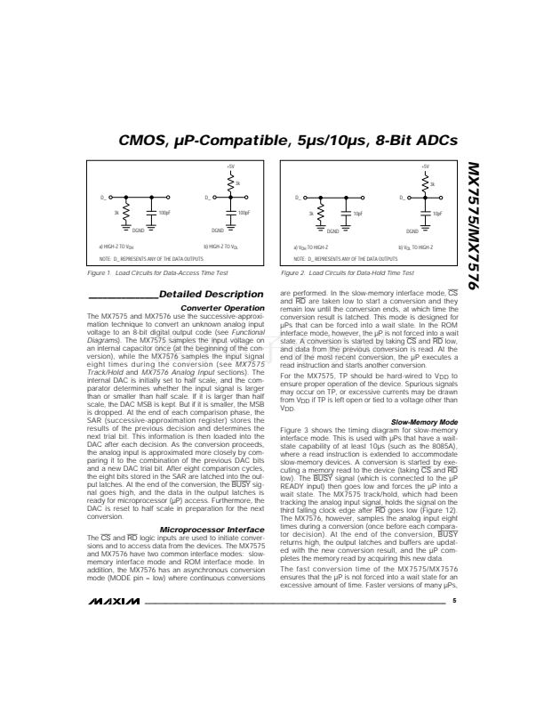
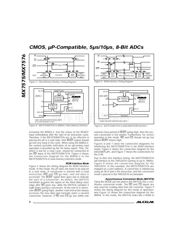
Figure 3. Slow-Memory Interface Timing Diagram
Figure 5. ROM Interface Timing Diagram
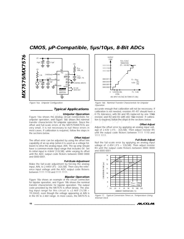
A8鈥揂15
ADDRESS BUS
+5V
TP/MODE
ADDRESS
DECODE
CS
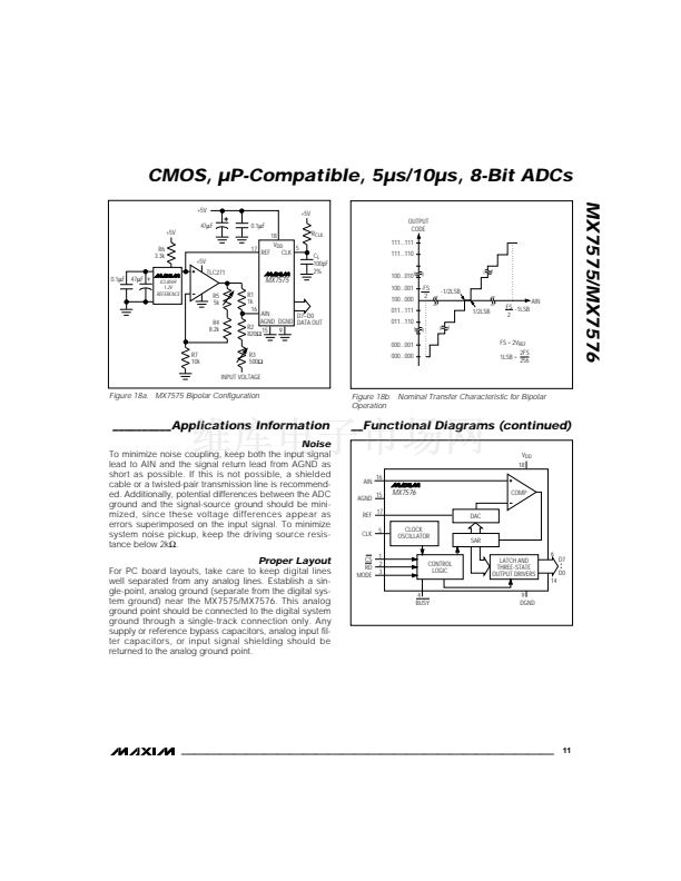
A0鈥揂15
ADDRESS BUS
+5V
TP/MODE
ADDRESS
EN DECODE
CS
RD
D0鈥揇7
8085A-2
S0
ALE
AD0鈥揂D7
READY
ADDRESS
LATCH
6502-6809
R/W
桅2
OR E
MX7575*
RD
MX7576
BUSY
D0鈥揇7
MX7575*
MX7576
DATA BUS
D0鈥揇7
DATA BUS
* SOME CIRCUITRY OMITTED FOR CLARITY
S0 IS LOW FOR READ CYCLES
* SOME CIRCUITRY OMITTED FOR CLARITY
Figure 4. MX7575/MX7576 to 8085A-2 Slow-Memory Interface
Figure 6. MX7575/MX7576 to 6502/6809 ROM Interface
including the 8085A-2, test the status of the READY
input immediately after the start of an instruction cycle.
Therefore, if the MX7575/MX7576 are to be effective in
placing the 碌P in a wait state, their
BUSY
output should
go low very early in the cycle. When using the 8085A-2,
the earliest possible indication of an upcoming read
operation is provided by the S0 status signal. Thus, S0,
which is low for a read cycle, should be connected to
the
RD
input of the MX7575/MX7576. Figure 4 shows
the connection diagram for the 8085A-2 to the
MX7575/MX7576 in slow-memory interface mode.
external clock period of
BUSY
going high, then the sec-
ond conversion is not started. Furthermore, for correct
operation in this mode,
RD
and
CS
should not go low
before
BUSY
returns high.
Figures 6 and 7 show the connection diagrams for
interfacing the MX7575/MX7576 in the ROM interface
mode. Figure 6 shows the connection diagram for the
6502/6809 碌Ps, and Figure 7 shows the connections for
the Z-80.
Due to their fast interface timing, the MX7575/MX7576
will interface to the TMS32010 running at up to 18MHz.
Figure 8 shows the connection diagram for the
TMS32010. In this example, the MX7575/MX7576 are
mapped as a port address. A conversion is initiated by
using an IN A and a PA instruction, and the conversion
result is placed in the TMS32010 accumulator.
ROM Interface Mode
Figure 5 shows the timing diagram for ROM interface
mode. In this mode, the 碌P does not need to be placed
in a wait state. A conversion is started with a read
instruction (RD and
CS
go low), and old data is
accessed. The
BUSY
signal then goes low to indicate
the start of a conversion. As before, the MX7575
track/hold acquires the signal on the third falling clock
edge after
RD
goes low, while the MX7576 samples it
eight times during a conversion. At the end of a conver-
sion (BUSY going high), another read instruction always
accesses the new data and normally starts a second
conversion. However, if
RD
and
CS
go low within one
6
Asynchronous Conversion Mode (MX7576)
Tying the MODE pin low places the MX7576 into a con-
tinuous conversion mode. The
RD
and
CS
inputs are
only used for reading data from the converter. Figure 9
shows the timing diagram for this mode of operation,
and Figure 10 shows the connection diagram for the
8085A. In this mode, the MX7576 looks like a ROM to
_______________________________________________________________________________________


 1
1
 2
2
 3
3
 4
4
 5
5
 6
6
 7
7
 8
8
 9
9
 10
10
 11
11
 12
12
