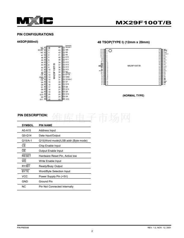
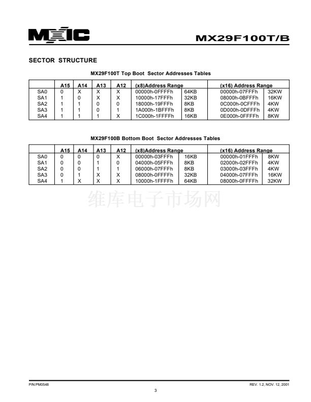
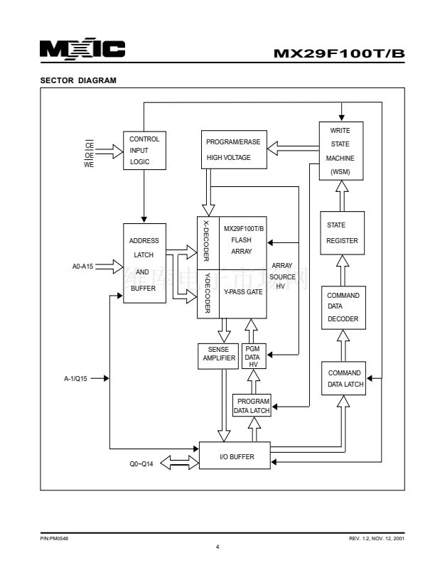
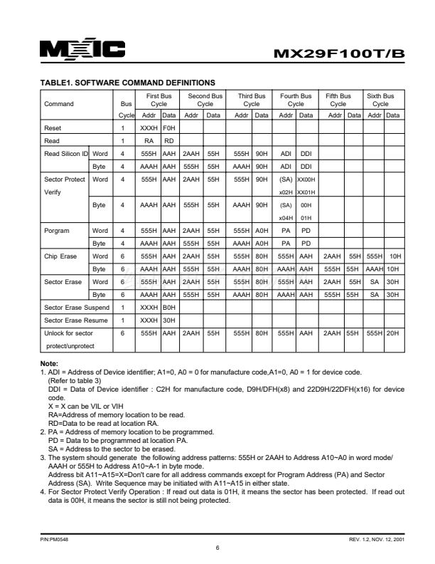
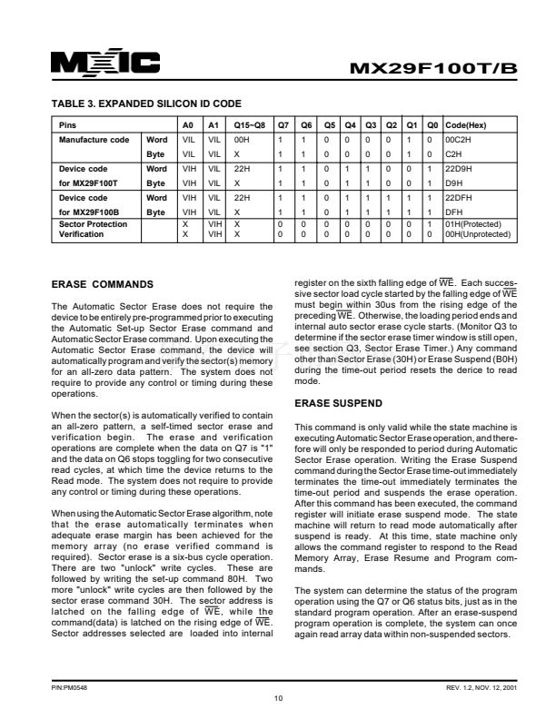
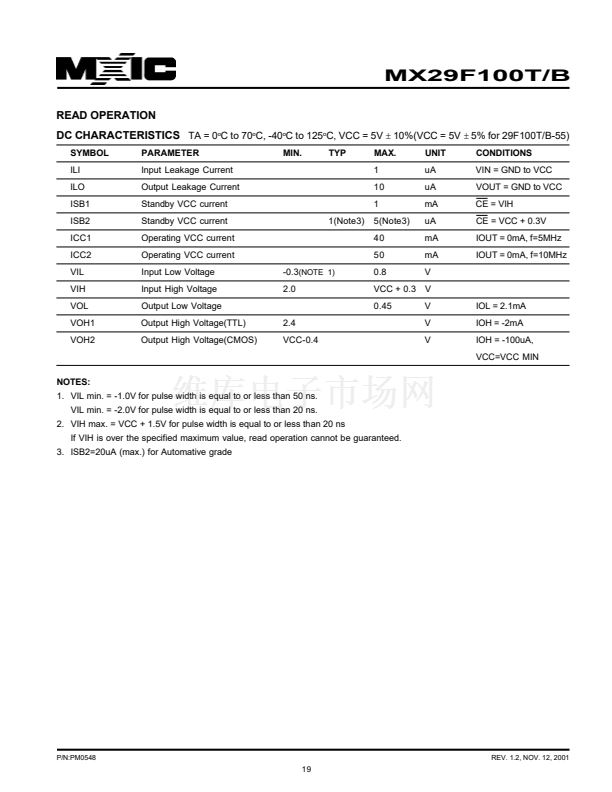
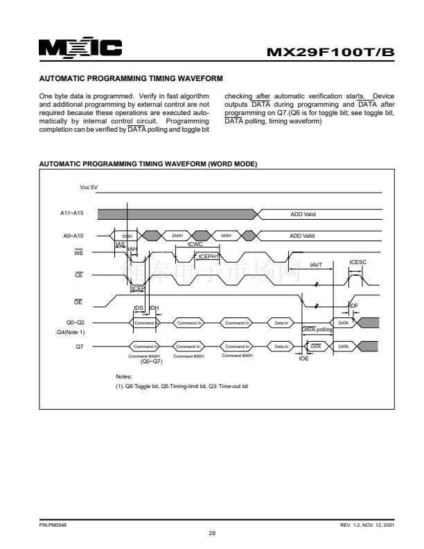
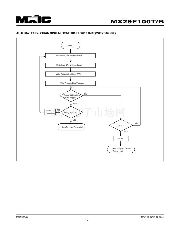
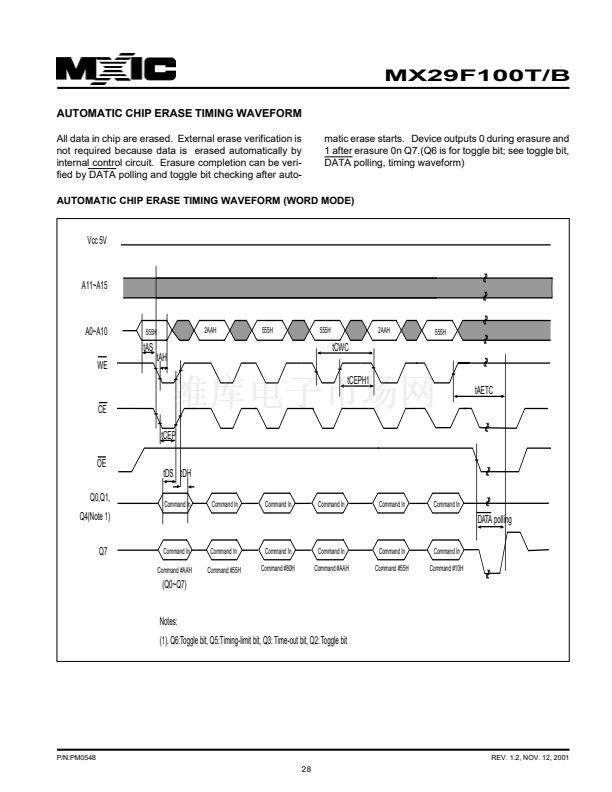
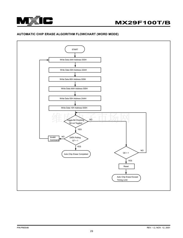
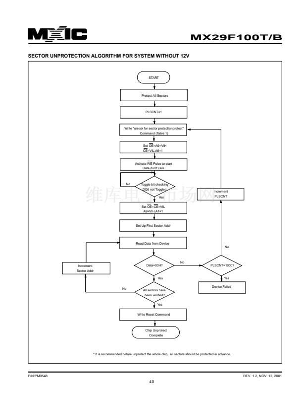
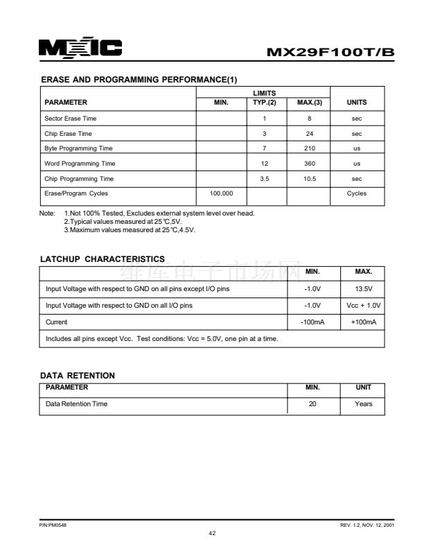
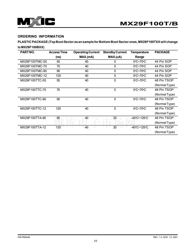
MX29F100T/B
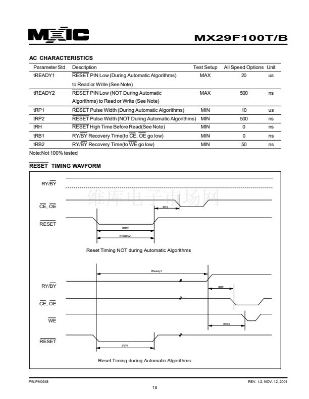
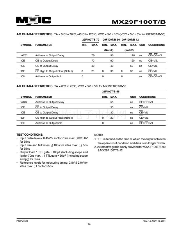
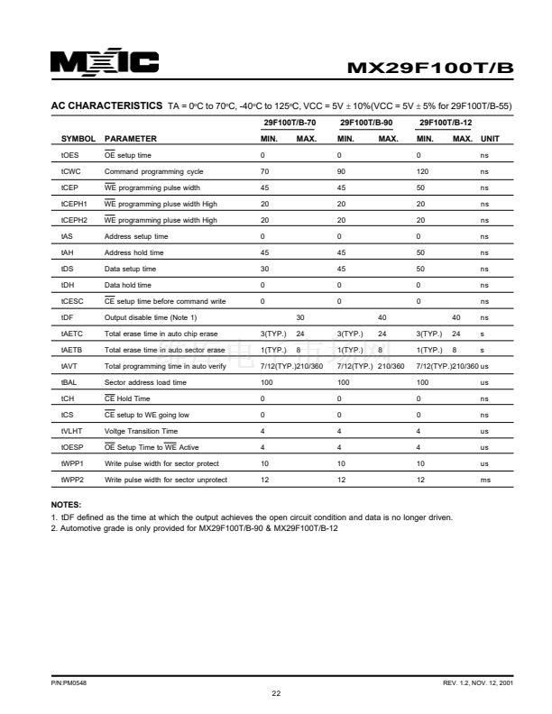
AC CHARACTERISTICS
TA = 0
o
C to 70
o
C, -40
o
C to 125
o
C, VCC = 5V
鹵
10%(VCC = 5V
鹵
5% for 29F100T/B-55)
29F100T/B-70
SYMBOL
PARAMETER
MIN.
MAX.
29F100T/B-90 29F100T/B-12
MIN.
MAX.
MIN.
MAX. UNIT
CONDITIONS
(Note2)
tACC
tCE
tOE
tDF
tOH
Address to Output Delay
CE to Output Delay
OE to Output Delay
OE High to Output Float
(
Note1)
Address to Output hold
0
0
70
70
40
20
0
0
90
90
40
30
0
0
(Note2)
120
120
50
30
ns
ns
ns
ns
ns
CE=OE=VIL
OE=VIL
CE=VIL
CE=VIL
CE=OE=VIL
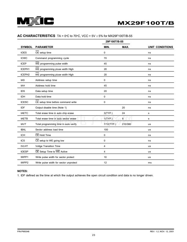
AC CHARACTERISTICS
TA = 0
o
C to 70
o
C, VCC = 5V
鹵
5% for MX29F100T/B-55
29F100T/B-55
SYMBOL
tACC
tCE
tOE
tDF
tOH
PARAMETER
Address to Output Delay
CE to Output Delay
OE to Output Delay
OE High to Output Float
(
Note1)
Address to Output hold
0
0
MIN.
MAX.
55
55
30
20
UNIT
ns
ns
ns
ns
ns
CONDITIONS
CE=OE=VIL
OE=VIL
CE=VIL
CE=VIL
CE=OE=VIL
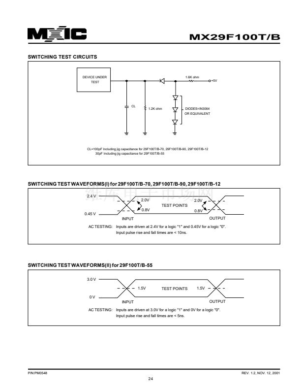
TEST CONDITIONS:
鈥?Input pulse levels: 0.45V/2.4V for 70ns max. ; 0V/3.0V
for 55ns
鈥?Input rise and fall times: < 10ns for 70ns max. ; < 5ns
for 55ns
鈥?Output load: 1 TTL gate + 100pF (Including scope and
jig) for 70ns max. ; 1 TTL gate + 30pF (Including scope
and jig) for 55ns
鈥?Reference levels for measuring timing: 0.8V & 2.0V for
70ns max. ; 1.5V for 55ns
NOTE:
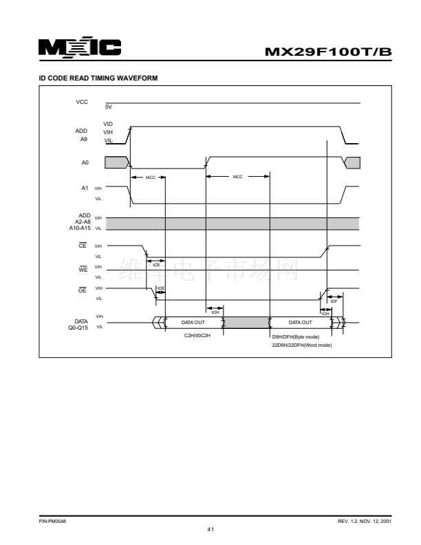
1. tDF is defined as the time at which the output achieves
the open circuit condition and data is no longer driven.
2. Automotive grade is only provided for MX29F100T/B-90
& MX29F100T/B-12
P/N:PM0548
REV. 1.2, NOV. 12, 2001
20


 1
1
 2
2
 3
3
 4
4
 5
5
 6
6
 7
7
 8
8
 9
9
 10
10
 11
11
 12
12
 13
13
 14
14
 15
15
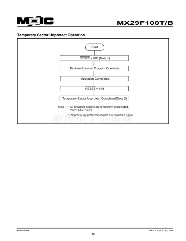 16
16
 17
17
 18
18
 19
19
 20
20
 21
21
 22
22
 23
23
 24
24
 25
25
 26
26
 27
27
 28
28
 29
29
 30
30
 31
31
 32
32
 33
33
 34
34
 35
35
 36
36
 37
37
 38
38
 39
39
 40
40
 41
41
 42
42
 43
43
 44
44
 45
45
 46
46
 47
47
