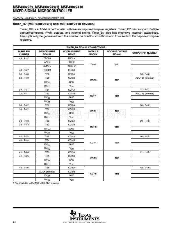
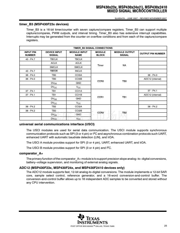
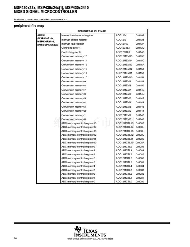
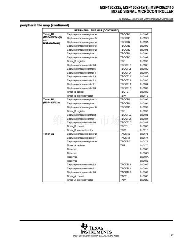
Stresses beyond those listed under 鈥渁bsolute maximum ratings鈥?may cause permanent damage to the device. These are stress ratings only, and
functional operation of the device at these or any other conditions beyond those indicated under 鈥渞ecommended operating conditions鈥?is not
implied. Exposure to absolute-maximum-rated conditions for extended periods may affect device reliability.
鈥?/div>
All voltages referenced to V . The JTAG fuse-blow voltage, V , is allowed to exceed the absolute maximum rating. The voltage is applied to
SS
FB
the TDI/TCLK pin when blowing the JTAG fuse.
摟
Higher temperature may be applied during board soldering process according to the current JEDEC J-STD-020 specification with peak reflow
temperatures not higher than classified on the device label on the shipping boxes or reels.
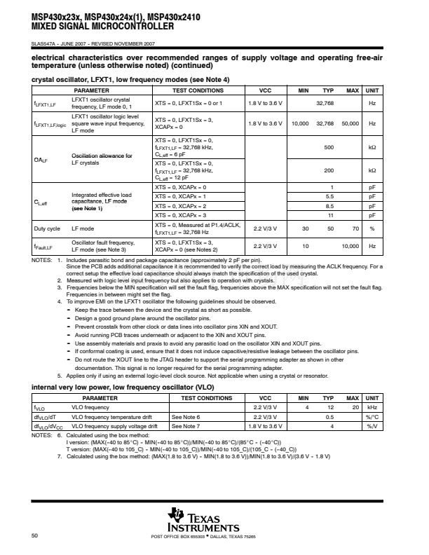
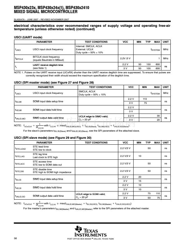
recommended operating conditions
PARAMETER
Supply voltage during program execution, V
CC
Supply voltage during flash memory programming, V
CC
Supply voltage, V
SS
Operating free air temperature range, T
A
free-air temperat re range
AV
CC
= DV
CC
= V
CC
(see Note 1)
AV
CC
= DV
CC
= V
CC
(see Note 1)
AV
SS
= DV
SS
= V
SS
I version
T version
V
CC
= 1.8 V,
Duty cycle = 50%
鹵
10%
Processor frequency f
SYSYTEM
(maximum MCLK frequency)
(see Notes 2 and 3 and Figure 1)
V
CC
= 2.7 V,
Duty cycle = 50%
鹵
10%
V
CC
鈮?/div>
3.3 V,
Duty cycle = 50%
鹵
10%
MIN
1.8
2.2
0.0
--40
--40
dc
dc
dc
MAX
3.6
3.6
0.0
85
105
4.15
12
16
MHz
UNITS
V
V
V
擄C
擄C
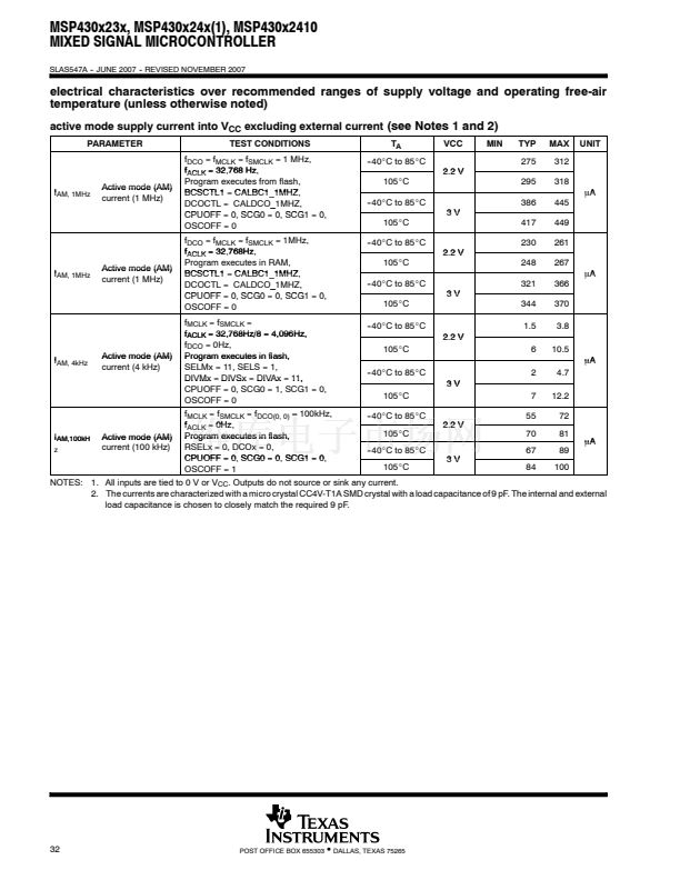
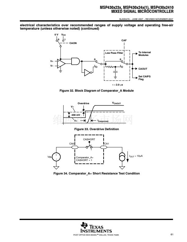
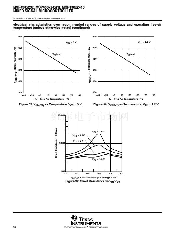
NOTES: 1. It is recommended to power AV
CC
and DV
CC
from the same source. A maximum difference of 0.3 V between AV
CC
and DV
CC
can
be tolerated during power-up.
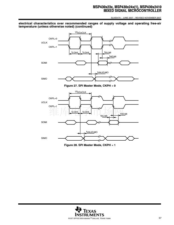
2. The MSP430 CPU is clocked directly with MCLK.
Both the high and low phase of MCLK must not exceed the pulse width of the specified maximum frequency.
3. Modules might have a different maximum input clock specification. See the specification of the respective module in this data sheet.
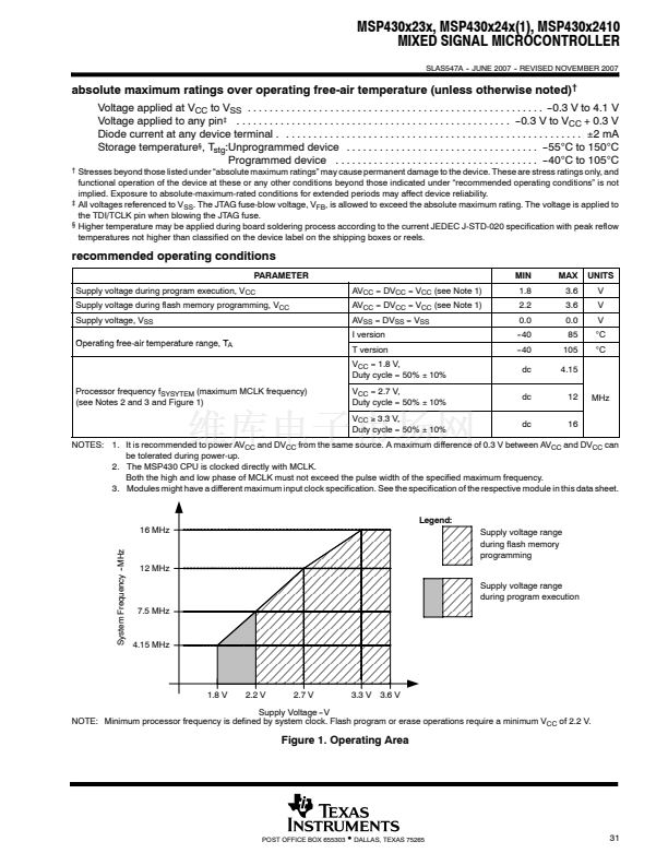
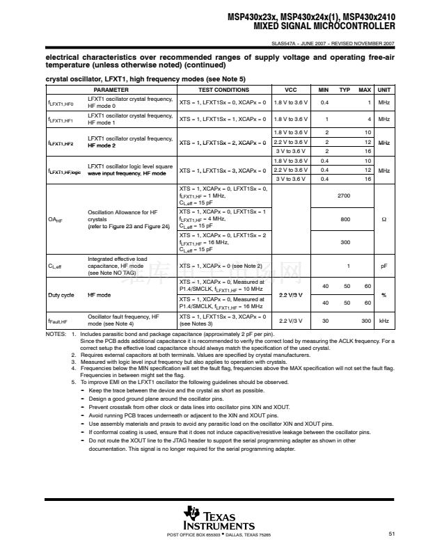
Legend:
Supply voltage range
during flash memory
programming
Supply voltage range
during program execution
7.5 MHz
16 MHz
System Frequency --MHz
12 MHz
4.15 MHz
1.8 V
2.2 V
2.7 V
3.3 V
3.6 V
Supply Voltage --V
NOTE: Minimum processor frequency is defined by system clock. Flash program or erase operations require a minimum V
CC
of 2.2 V.
Figure 1. Operating Area
POST OFFICE BOX 655303
鈥?/div>
DALLAS, TEXAS 75265
31


 1
1
 2
2
 3
3
 4
4
 5
5
 6
6
 7
7
 8
8
 9
9
 10
10
 11
11
 12
12
 13
13
 14
14
 15
15
 16
16
 17
17
 18
18
 19
19
 20
20
 21
21
 22
22
 23
23
 24
24
 25
25
 26
26
 27
27
 28
28
 29
29
 30
30
 31
31
 32
32
 33
33
 34
34
 35
35
 36
36
 37
37
 38
38
 39
39
 40
40
 41
41
 42
42
 43
43
 44
44
 45
45
 46
46
 47
47
 48
48
 49
49
 50
50
 51
51
 52
52
 53
53
 54
54
 55
55
 56
56
 57
57
 58
58
 59
59
 60
60
 61
61
 62
62
 63
63
 64
64
 65
65
 66
66
 67
67
 68
68
 69
69
 70
70
 71
71
 72
72
 73
73
 74
74
 75
75
 76
76
 77
77
 78
78
 79
79
 80
80
 81
81
 82
82
 83
83
 84
84
 85
85
 86
86
 87
87
 88
88
 89
89
 90
90
 91
91
