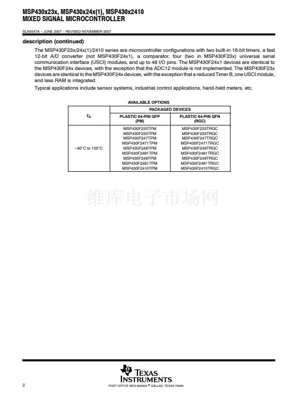
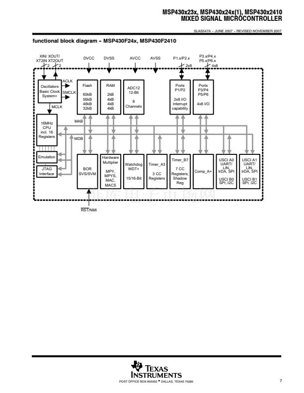
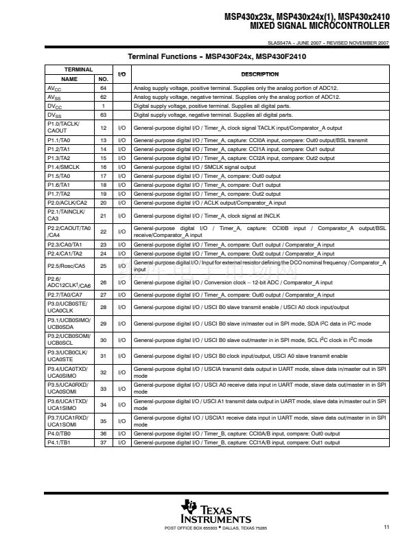
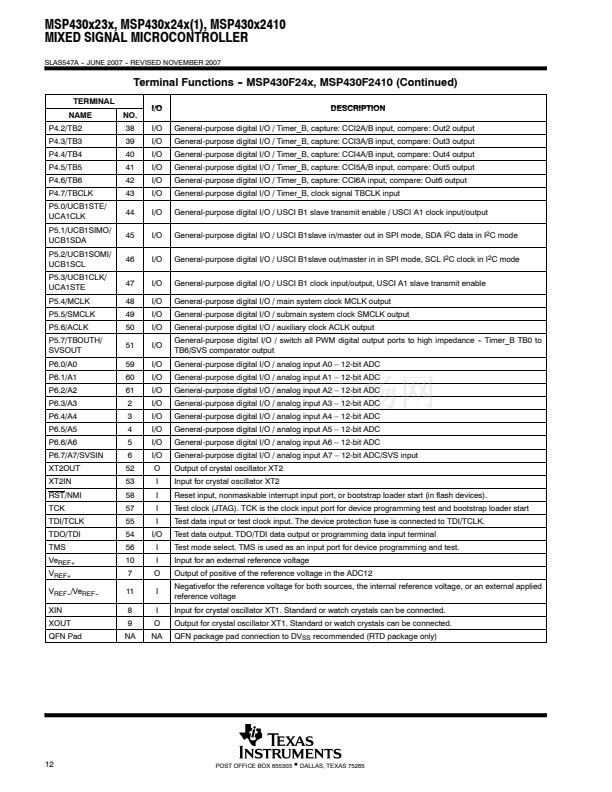
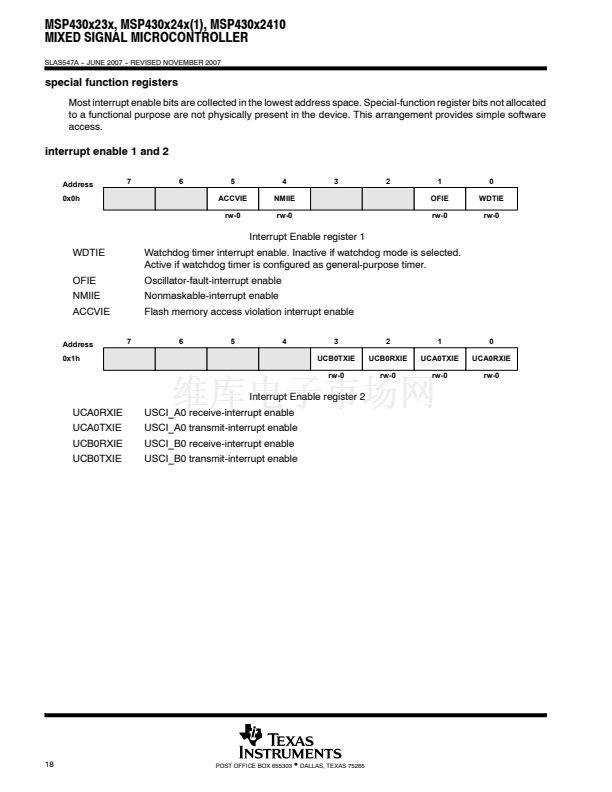
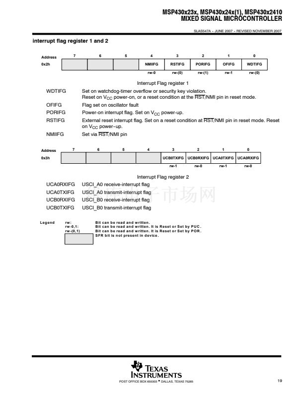
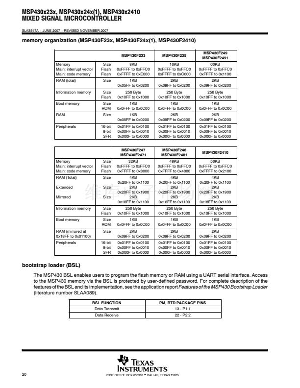
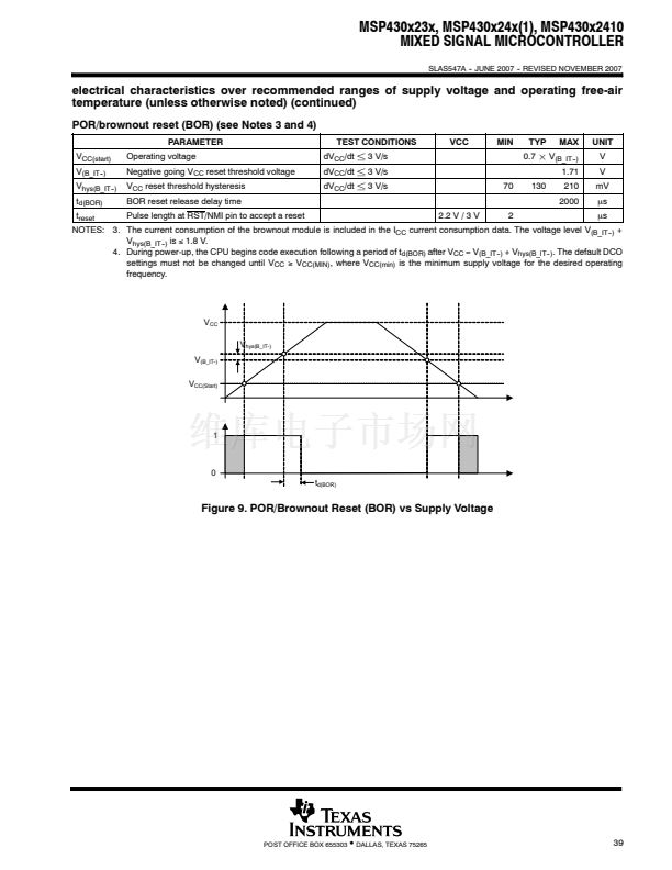
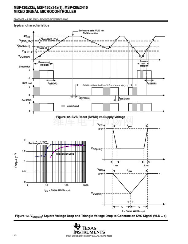
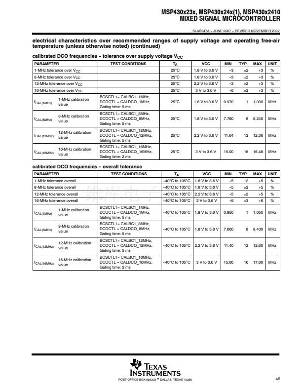
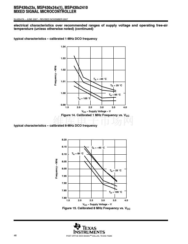
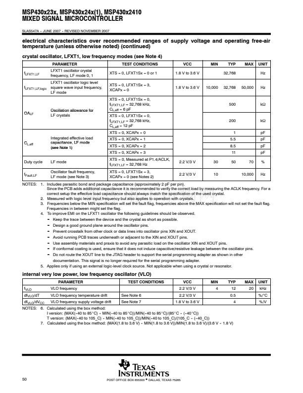
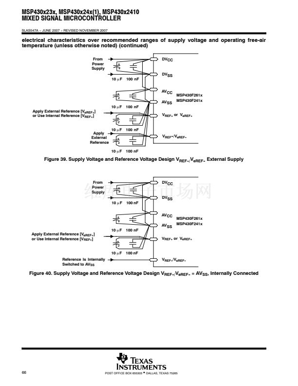
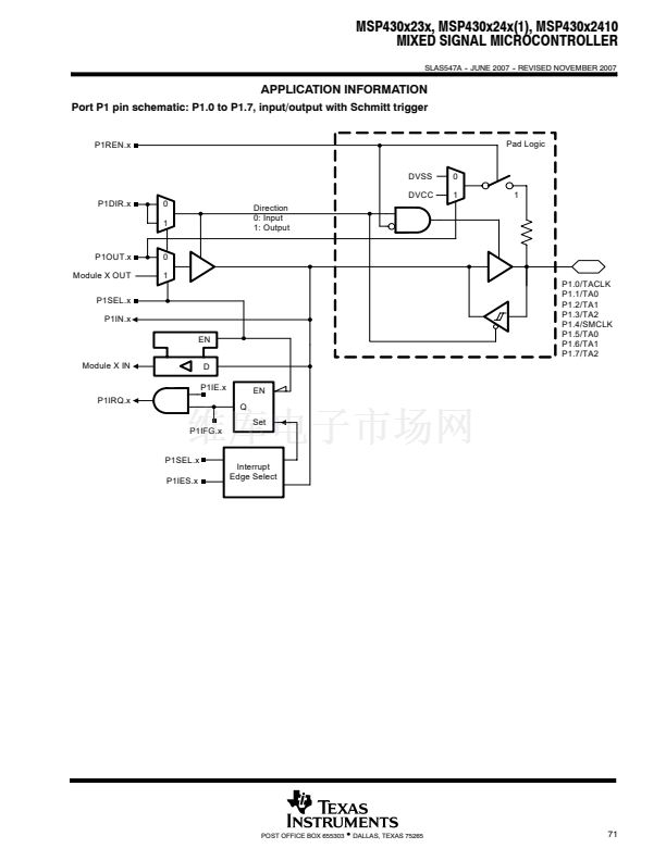
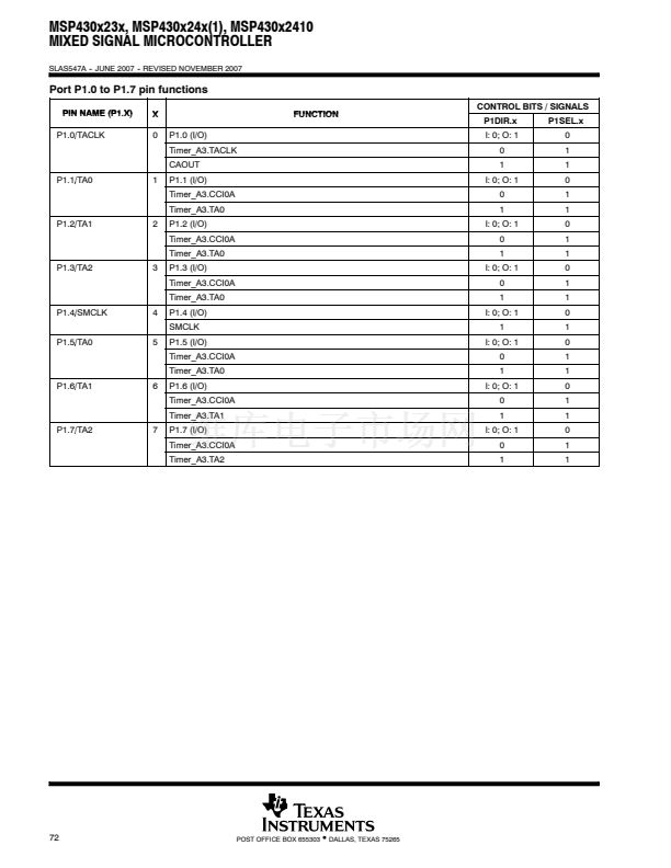
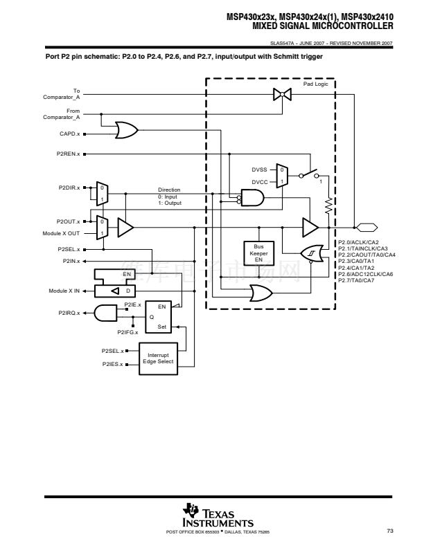
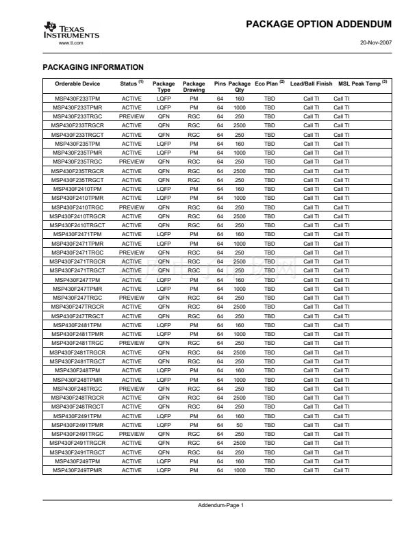
MSP430x23x, MSP430x24x(1), MSP430x2410
MIXED SIGNAL MICROCONTROLLER
SLAS547A -- JUNE 2007 -- REVISED NOVEMBER 2007
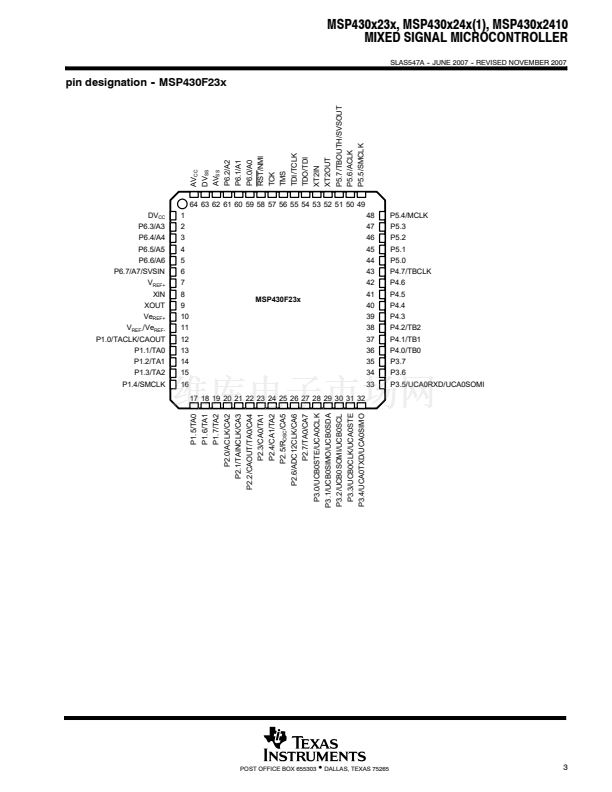
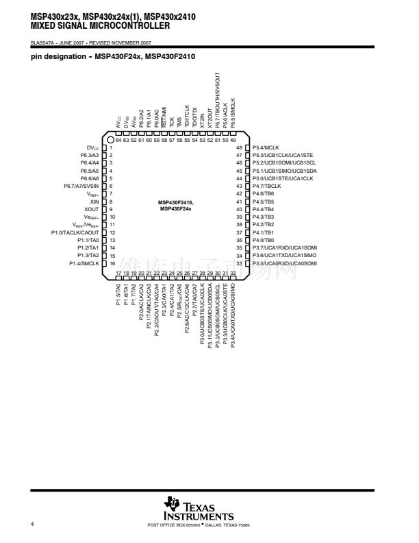
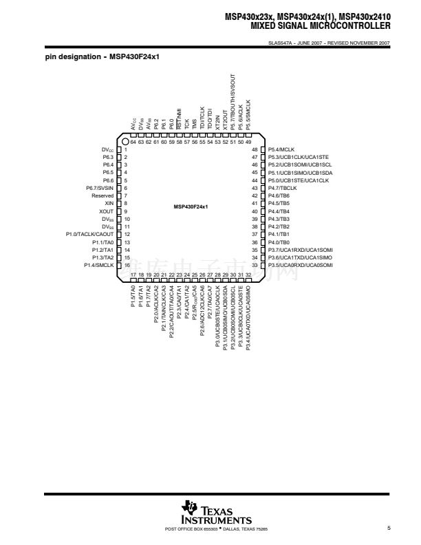
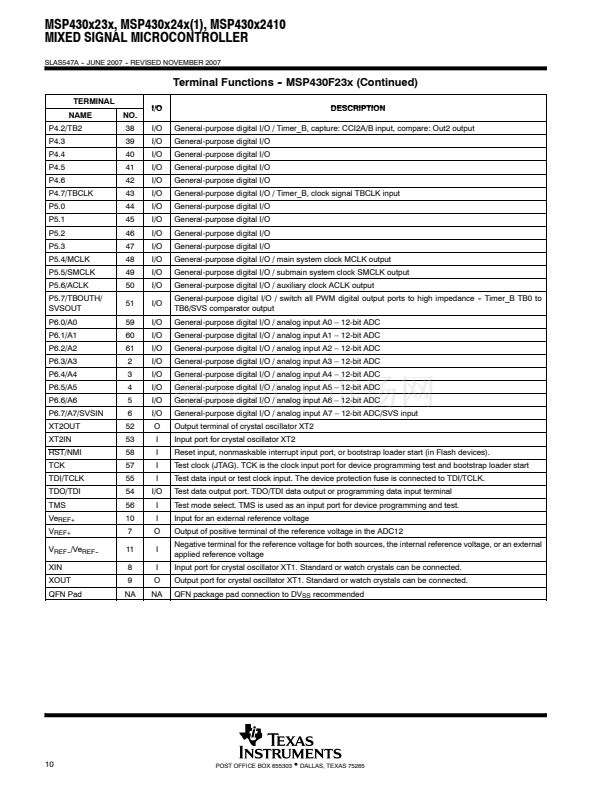
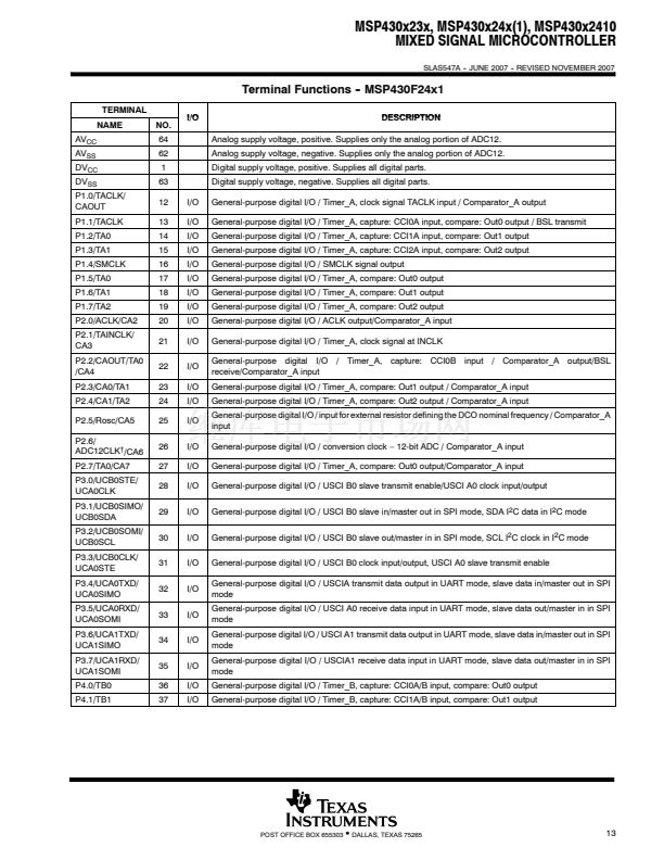
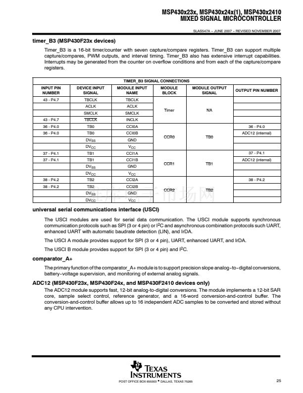
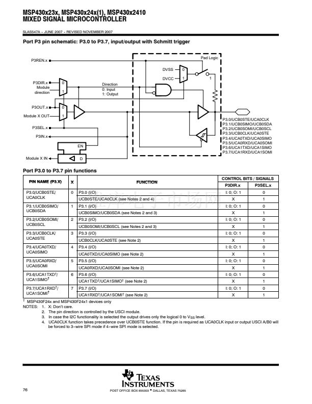
Terminal Functions - MSP430F23x (Continued)
-
TERMINAL
NAME
P4.2/TB2
P4.3
P4.4
P4.5
P4.6
P4.7/TBCLK
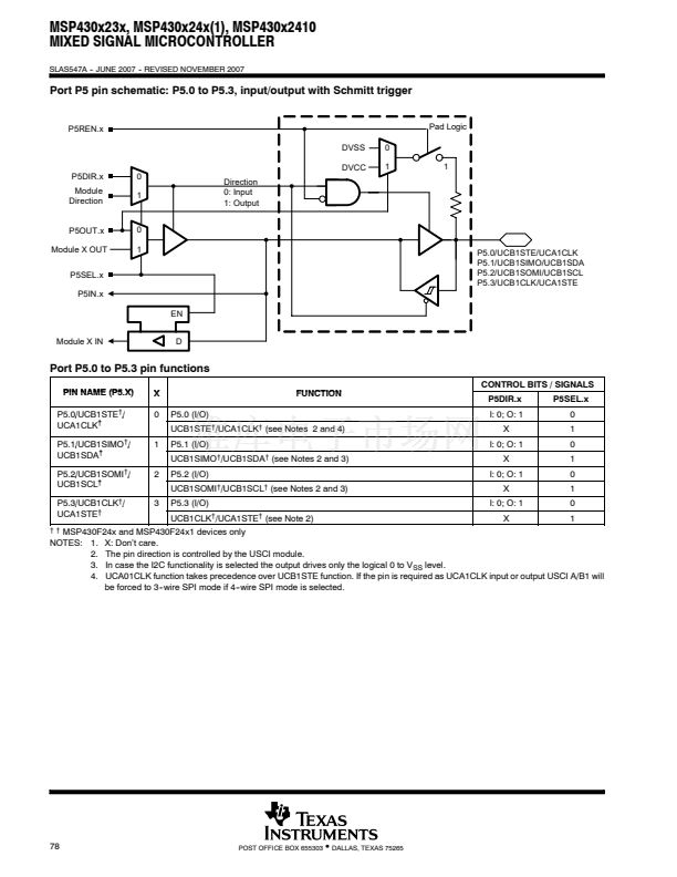
P5.0
P5.1
P5.2
P5.3
P5.4/MCLK
P5.5/SMCLK
P5.6/ACLK
P5.7/TBOUTH/
SVSOUT
P6.0/A0
P6.1/A1
P6.2/A2
P6.3/A3
P6.4/A4
P6.5/A5
P6.6/A6
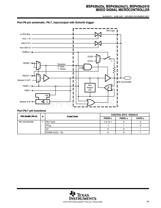
P6.7/A7/SVSIN
XT2OUT
XT2IN
RST/NMI
TCK
TDI/TCLK
TDO/TDI
TMS
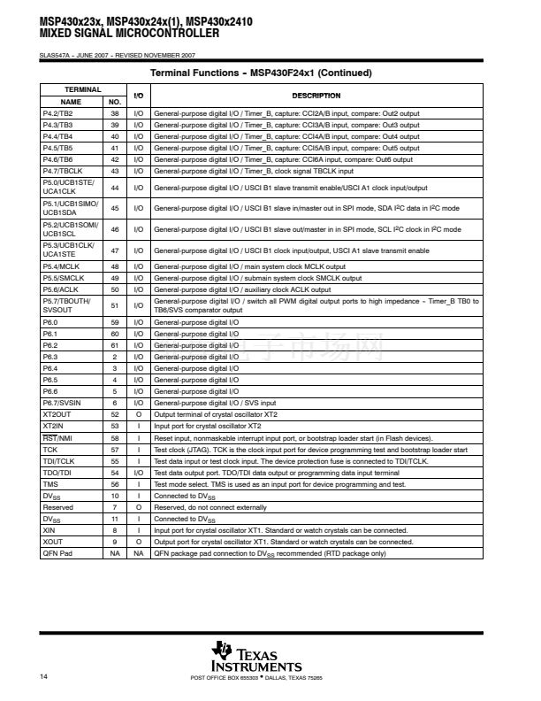
Ve
REF+
V
REF+
V
REF--
/Ve
REF--
XIN
XOUT
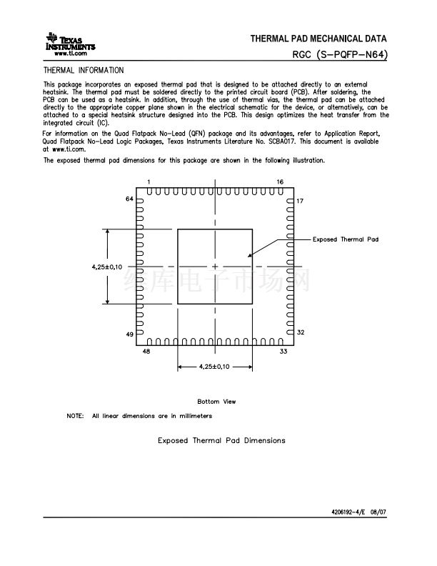
QFN Pad
NO.
38
39
40
41
42
43
44
45
46
47
48
49
50
51
59
60
61
2
3
4
5
6
52
53
58
57
55
54
56
10
7
11
8
9
NA
I/O
I/O
I/O
I/O
I/O
I/O
I/O
I/O
I/O
I/O
I/O
I/O
I/O
I/O
I/O
I/O
I/O
I/O
I/O
I/O
I/O
I/O
I/O
O
I
I
I
I
I/O
I
I
O
I
I
O
NA
DESCRIPTION
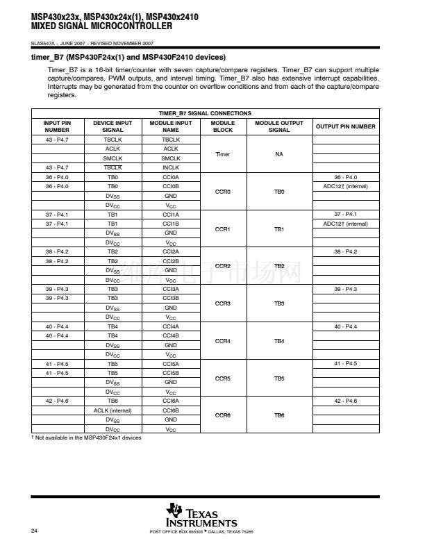
General-purpose digital I/O / Timer_B, capture: CCI2A/B input, compare: Out2 output
General-purpose digital I/O
General-purpose digital I/O
General-purpose digital I/O
General-purpose digital I/O
General-purpose digital I/O / Timer_B, clock signal TBCLK input
General-purpose digital I/O
General-purpose digital I/O
General-purpose digital I/O
General-purpose digital I/O
General-purpose digital I/O / main system clock MCLK output
General-purpose digital I/O / submain system clock SMCLK output
General-purpose digital I/O / auxiliary clock ACLK output
General-purpose digital I/O / switch all PWM digital output ports to high impedance -- Timer_B TB0 to
TB6/SVS comparator output
General-purpose digital I/O / analog input A0 鈥?12-bit ADC
General-purpose digital I/O / analog input A1 鈥?12-bit ADC
General-purpose digital I/O / analog input A2 鈥?12-bit ADC
General-purpose digital I/O / analog input A3 鈥?12-bit ADC
General-purpose digital I/O / analog input A4 鈥?12-bit ADC
General-purpose digital I/O / analog input A5 鈥?12-bit ADC
General-purpose digital I/O / analog input A6 鈥?12-bit ADC
General-purpose digital I/O / analog input A7 鈥?12-bit ADC/SVS input
Output terminal of crystal oscillator XT2
Input port for crystal oscillator XT2
Reset input, nonmaskable interrupt input port, or bootstrap loader start (in Flash devices).
Test clock (JTAG). TCK is the clock input port for device programming test and bootstrap loader start
Test data input or test clock input. The device protection fuse is connected to TDI/TCLK.
Test data output port. TDO/TDI data output or programming data input terminal
Test mode select. TMS is used as an input port for device programming and test.
Input for an external reference voltage
Output of positive terminal of the reference voltage in the ADC12
Negative terminal for the reference voltage for both sources, the internal reference voltage, or an external
applied reference voltage
Input port for crystal oscillator XT1. Standard or watch crystals can be connected.
Output port for crystal oscillator XT1. Standard or watch crystals can be connected.
QFN package pad connection to DV
SS
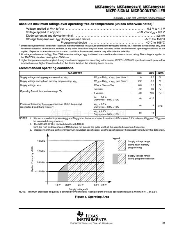
recommended
10
POST OFFICE BOX 655303
鈥?/div>
DALLAS, TEXAS 75265


 1
1
 2
2
 3
3
 4
4
 5
5
 6
6
 7
7
 8
8
 9
9
 10
10
 11
11
 12
12
 13
13
 14
14
 15
15
 16
16
 17
17
 18
18
 19
19
 20
20
 21
21
 22
22
 23
23
 24
24
 25
25
 26
26
 27
27
 28
28
 29
29
 30
30
 31
31
 32
32
 33
33
 34
34
 35
35
 36
36
 37
37
 38
38
 39
39
 40
40
 41
41
 42
42
 43
43
 44
44
 45
45
 46
46
 47
47
 48
48
 49
49
 50
50
 51
51
 52
52
 53
53
 54
54
 55
55
 56
56
 57
57
 58
58
 59
59
 60
60
 61
61
 62
62
 63
63
 64
64
 65
65
 66
66
 67
67
 68
68
 69
69
 70
70
 71
71
 72
72
 73
73
 74
74
 75
75
 76
76
 77
77
 78
78
 79
79
 80
80
 81
81
 82
82
 83
83
 84
84
 85
85
 86
86
 87
87
 88
88
 89
89
 90
90
 91
91
