鈩?/div>
, 2W
load resistor.
4.7碌F
MIC5018
2
4
VS
CTL
G
GND
3
1
Figure 6. 12V High-Side Switch
A logic-level MOSFET is required. The MOSFET鈥檚 maximum
current is limited slightly because the gate is not fully en-
hanced. To predict the MOSFETs performance for any pair
of supply voltages, calculate the gate-to-source voltage and
refer to the MOSFET data sheet.
V
GS
= V
G
鈥?(V
LOAD SUPPLY
鈥?V
DS
)
V
G
is determined from the driver supply voltage using the
鈥淭ypical Characteristics: Gate Output Voltage vs. Supply
Voltage鈥?graph.
Low-Side Switch Configuration
The low-side configuration makes it possible to switch a
voltage much higher than the MIC5018鈥檚 maximum supply
voltage.
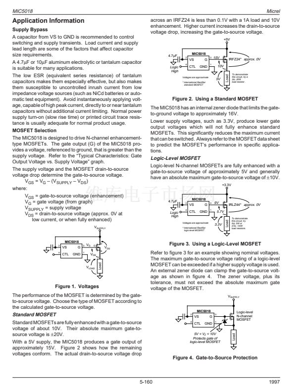
+80V
* International Rectifier
standard MOSFET
BV
DSS
= 100V
To demonstrate
this circuit, try
1k, 10W or
33k, 1/4W
load resistors.
On
Off
Schottky
Diode
Figure 5. Switching an Inductive Load
Switching off an inductive load in a high-side application
momentarily forces the MOSFET source negative (as the
inductor opposes changes to current). This voltage spike can
be very large and can exceed a MOSFET鈥檚 gate-to-source
and drain-to-source ratings. A Schottky diode across the
inductive load provides a discharge current path to minimize
the voltage spike. The peak current rating of the diode should
be greater than the load current.
In a low-side application, switching off an inductive load will
momentarily force the MOSFET drain higher than the supply
voltage. The same precaution applies.
Load
5
+2.7 to +9V
4.7碌F
MIC5018
2
4
On
Off
3
1
Load
G
VS
CTL
GND
IRF540*
N-channel
MOSFET
Figure 7. Low-Side Switch Configuration
The maximum switched voltage is limited only by the
MOSFET鈥檚 maximum drain-to-source ratings.
1997
5-161


 1
1
 2
2
 3
3
 4
4
 5
5
 6
6
 7
7
