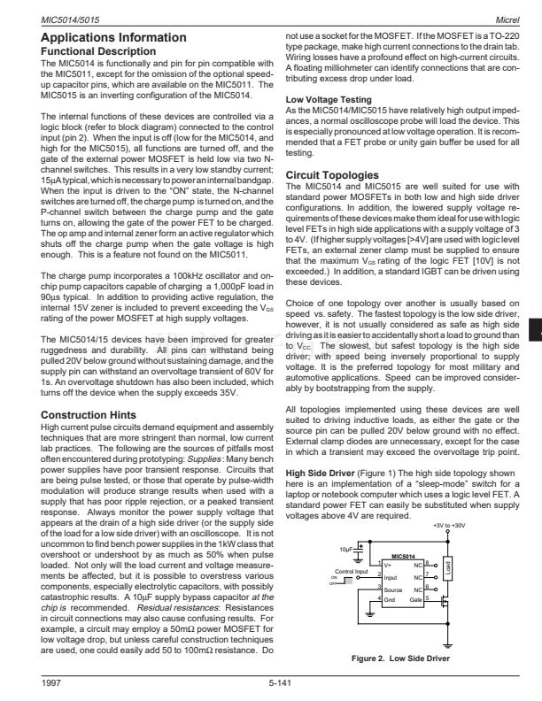
鈮?/div>
30V
V
+
= 4.5V
C
L
= 1000pF
V
+
= 12V
C
L
= 1000pF
V
+
= 4.5V
C
L
= 1000pF
V
+
= 12V
C
L
= 1000pF
+
unless otherwise specified
Conditions
Min
Typ
V
IN
De-Asserted (Note 5)
10
V
IN
Asserted (Note 5)
5.0
V
IN
De-Asserted
10
V
IN
Asserted
60
V
IN
De-Asserted
10
V
IN
Asserted
25
Digital Low Level
Digital High Level
2.0
V
IN
Low
鈥?.0
0
V
IN
High
1.0
V
IN
Low
鈥?.0
鈥?.0
V
IN
High
鈥?.0
5.0
V
IN
Asserted
4.0
V
IN
Asserted
13
15
2.5
90
6.0
6.0
35
37
Max
25
10
25
100
25
35
0.8
Units
碌A(chǔ)
mA
碌A(chǔ)
碌A(chǔ)
V
碌A(chǔ)
碌A(chǔ)
pF
V
V
ms
碌s
碌s
碌s
V
2.0
2.0
17
17
8.0
140
30
30
41
5
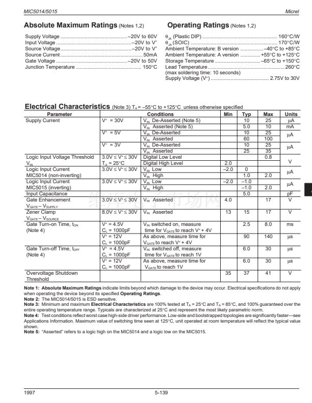
Gate Turn-off Time, t
OFF
(Note 4)
V
IN
switched on, measure
time for V
GATE
to reach V
+
+ 4V
As above, measure time for
V
GATE
to reach V
+
+ 4V
V
IN
switched off, measure
time for V
GATE
to reach 1V
As above, measure time for
V
GATE
to reach 1V
Overvoltage Shutdown
Threshold
Note 1: Absolute Maximum Ratings
indicate limits beyond which damage to the device may occur. Electrical specifications do not apply
when operating the device beyond its specified
Operating Ratings.
Note 2:
The MIC5014/5015 is ESD sensitive.
Note 3:
Minimum and maximum
Electrical Characteristics
are 100% tested at T
A
= 25擄C and T
A
= 85擄C, and 100% guaranteed over the
entire operating temperature range. Typicals are characterized at 25擄C and represent the most likely parametric norm.
Note 4:
Test conditions reflect worst case high-side driver performance. Low-side and bootstrapped topologies are significantly faster鈥攕ee
Applications Information. Maximum value of switching time seen at 125擄C, unit operated at room temperature will reflect the typical value
shown.
Note 5:
鈥淎sserted鈥?refers to a logic high on the MIC5014 and a logic low on the MIC5015.
1997
5-139


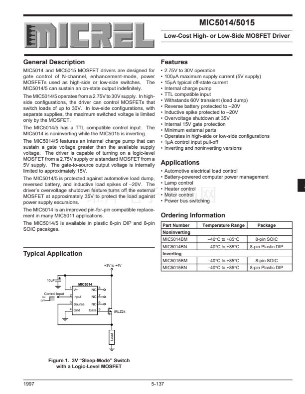 1
1
 2
2
 3
3
 4
4
 5
5
 6
6
 7
7
 8
8
 9
9
