500鈩?/div>
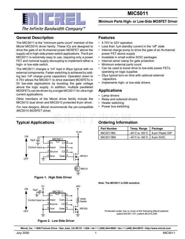
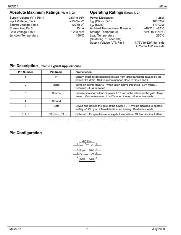
5 Gate
12.5V
Input 2
LOGIC
3 Source
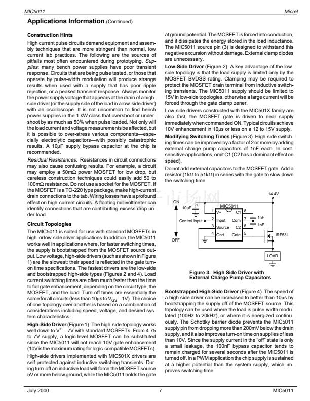
Applications Information
Functional Description (Refer to Block Diagram)
The MIC5011 functions are controlled via a logic block
connected to the input pin 2. When the input is low, all
functions are turned off for low standby current and the gate
of the power MOSFET is also held low through 500鈩?to an
N-channel switch. When the input is taken above the turn-
on threshold (3.5V typical), the N-channel switch turns off
and the charge pump is turned on to charge the gate of the
power FET.
MIC5011
6
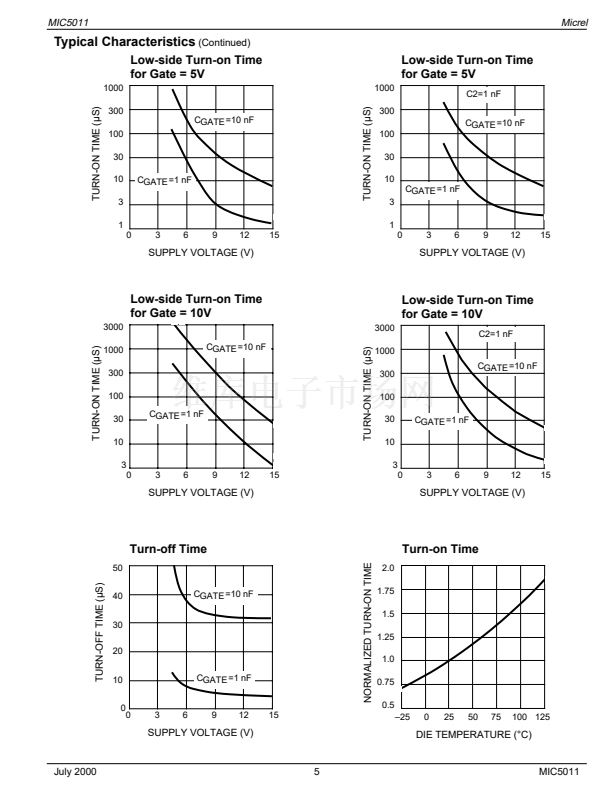
The charge pump incorporates a 100kHz oscillator and on-
chip pump capacitors capable of charging 1nF to 5V above
supply in 60碌s typical. With the addition of 1nF capacitors
at C1 and C2, the turn-on time is reduced to 25碌s typical
(see Figure 3). The charge pump is capable of pumping the
gate up to over twice the supply voltage. For this reason, a
zener clamp (12.5V typical) is provided between the gate
pin 5 and source pin 3 to prevent exceeding the V
GS
rating
of the MOSFET at high supplies.
July 2000


 1
1
 2
2
 3
3
 4
4
 5
5
 6
6
 7
7
 8
8
 9
9
 10
10
 11
11
 12
12
