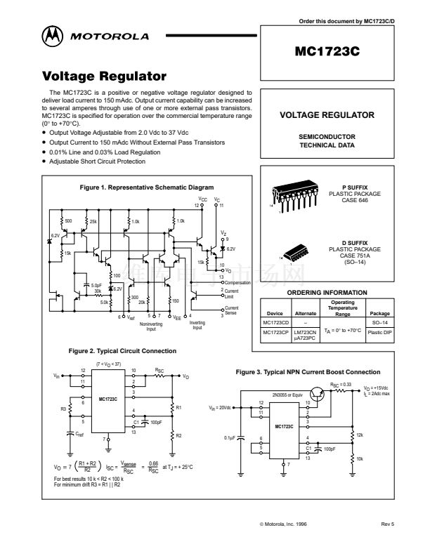
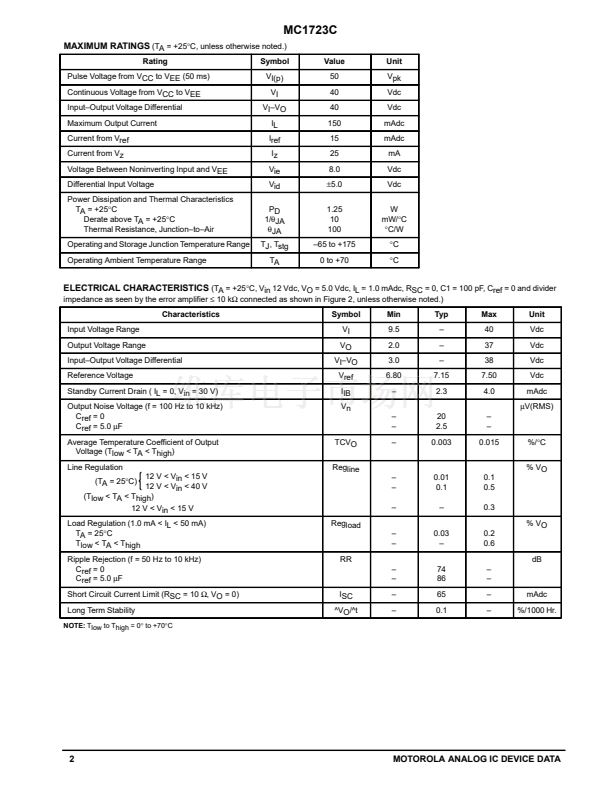
MC1723C
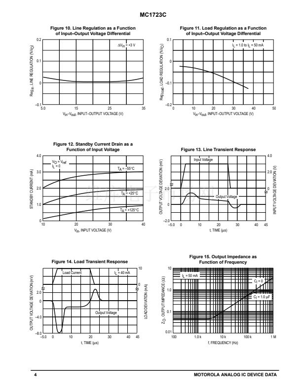
Figure 10. Line Regulation as a Function
of Input鈥揙utput Voltage Differential
0.2
Reg load , LOAD REGULATION (%VO )
Reg in , LINE REGULATION (%VO )
鈭哣
in = +3 V
0.1
IL = 1.0 to IL = 50 mA
Figure 11. Load Regulation as a Function
of Input鈥揙utput Voltage Differential
0.1
0
0
鈥?.1
鈥?.1
5.0
15
25
Vin鈥揤out, INPUT鈥揙UTPUT VOLTAGE (V)
35
鈥?.2
0
10
20
30
40
Vin鈥揤out, INPUT鈥揙UTPUT VOLTAGE (V)
50
Figure 12. Standby Current Drain as a
Function of Input Voltage
4.0
VO = Vref
IL = 0
STANDBY CURRENT (mA)
3.0
OUTPUT VOLTAGE DEVIATION (mV)
Figure 13. Line Transient Response
4.0
Input Voltage
2.0
INPUT VOLTAGE DEVIATION (V)
TA = 鈥?5擄C
2.0
TA = +25擄C
1.0
TA = +125擄C
0
10
20
30
Vin, INPUT VOLTAGE (V)
40
2.0
Output Voltage
0
0
鈥?.0
鈥?.0
0
10
20
t, TIME (碌s)
30
40
45
Figure 14. Load Transient Response
10
Load Current
OUTPUT VOLTAGE DEVIATION (mV)
IL = 40 mA
Z O , OUTPUT IMPEDANCE (
鈩?/div>
)
LOAD DEVIATION (mA)
0
2.0
0
Output Voltage
鈥?.0
10
Figure 15. Output Impedance as
Function of Frequency
IL = 50 mA
CI = 0
1.0
CI = 1.0
碌F
0.1
鈥?.0
鈥?.0
0
10
20
t, TIME (碌s)
30
40
45
0.01
100
1.0 k
10 k
f, FREQUENCY (Hz)
100 k
1M
4
MOTOROLA ANALOG IC DEVICE DATA


 1
1
 2
2
 3
3
 4
4
 5
5
 6
6
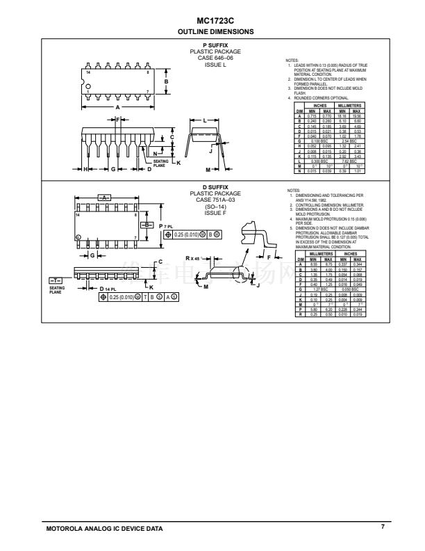 7
7
 8
8
