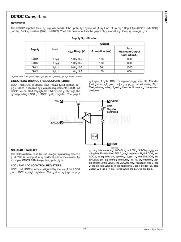
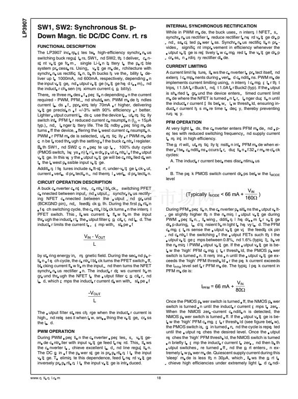
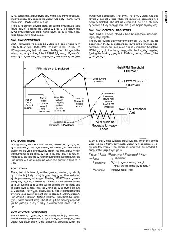
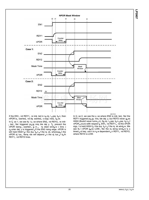
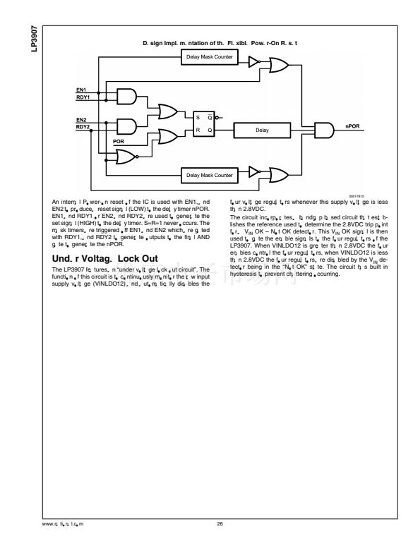
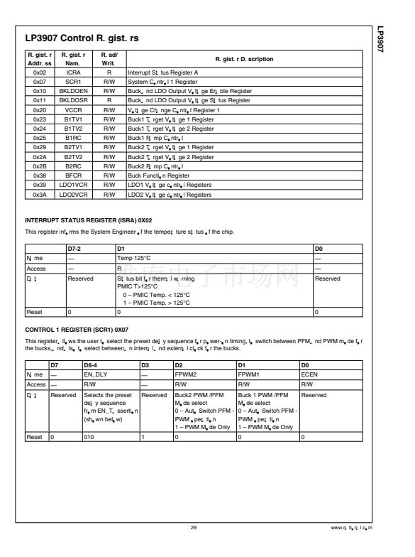
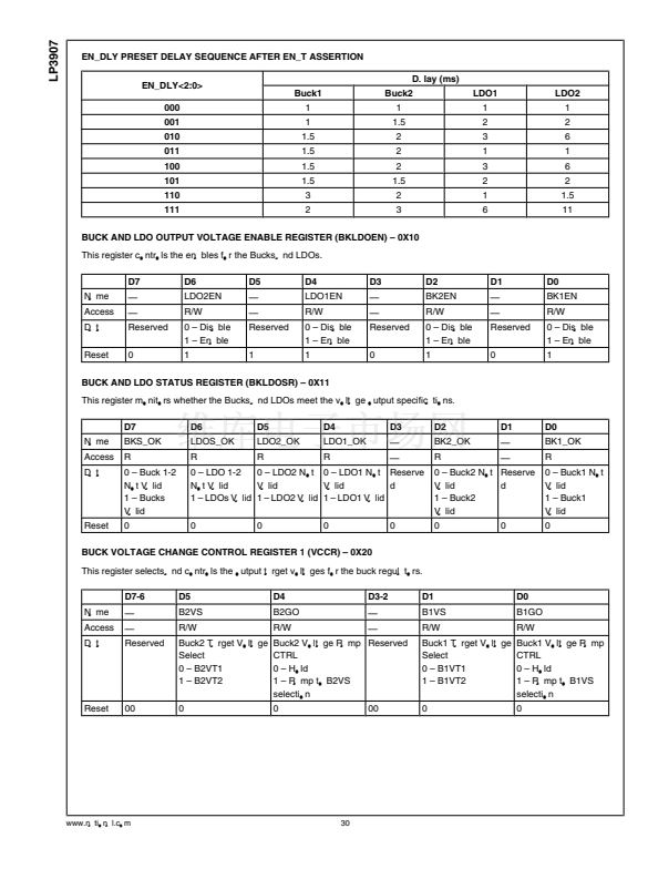
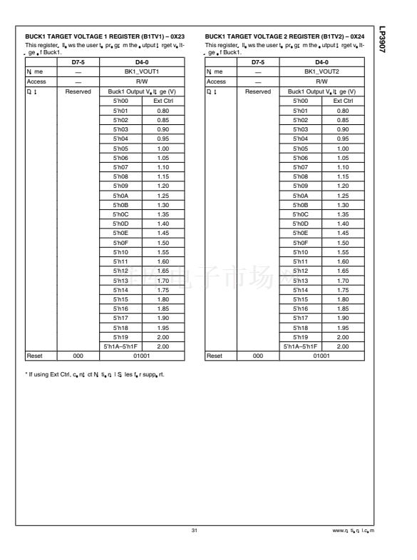
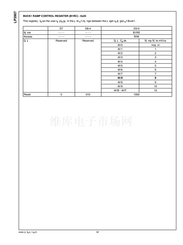
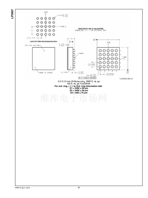
LP3907
I/O Electrical Characteristics
Unless otherwise noted: Typical values and limits appearing in normal type apply for T
J
= 25擄C. Limits appearing in
boldface
type
apply over the entire junction temperature range for operation, T
J
= 0擄C to +125擄C. (Note 13)
Symbol
V
IL
V
IH
Parameter
Input Low Level
Input High Level
1.2
Conditions
Limit
Min
Max
0.4
Units
V
V
Power On Reset Threshold/Function (POR)
Symbol
nPOR
nPOR
threshold
VOL
Parameter
nPOR = Power on reset forBuck1 and
Buck2
Percentage of Target voltage Buck1 or
Buck2
Output Level Low
Default
V
BUCK1
AND V
BUCK2
rising
V
BUCK1
OR V
BUCK2
falling
Load = IoL = 500mA
Conditions
Min
Typ
50
94
85
0.23
0.5
Max
Units
ms
%
V
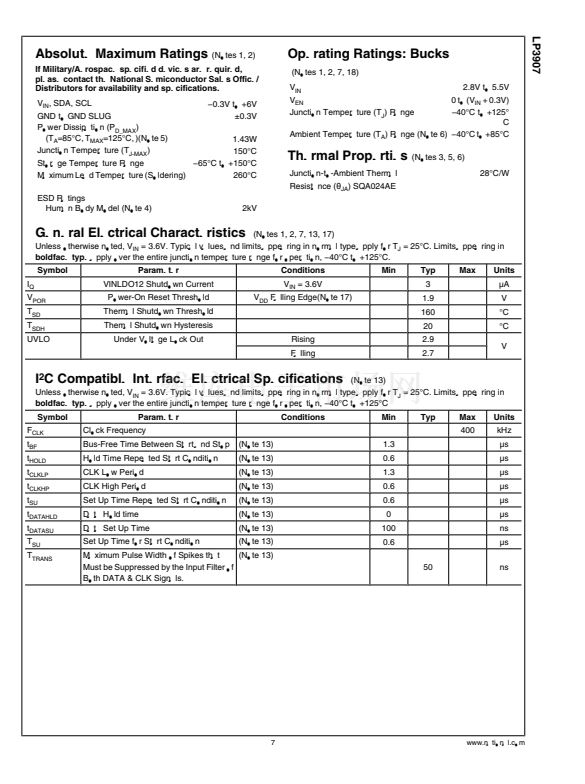
Note 1:
Absolute Maximum Ratings indicate limits beyond which damage to the component may occur. Operating Ratings are conditions under which operation
of the device is guaranteed. Operating Ratings do not imply guaranteed performance limits. For guaranteed performance limits and associated test conditions,
see the Electrical Characteristics.
Note 2:
All voltages are with respect to the potential at the GND pin.
Note 3:
Internal thermal shutdown circuitry protects the device from permanent damage. Thermal shutdown engages at T
J
= 160擄C (typ.) and disengages at T
J
= 140擄C (typ.)
Note 4:
The Human body model is a 100pF capacitor discharged through a 1.5k鈩?resistor into each pin. (MILSTD - 883 3015.7)
Note 5:
In applications where high power dissipation and/or poor package thermal resistance is present, the maximum ambient temperature may have to be
derated. Maximum ambient temperature (T
A-MAX
) is dependent on the maximum operating junction temperature (T
J-MAX-OP
= 125擄C), the maximum power
dissipation of the device in the application (P
D-MAX
), and the junction-to-ambient thermal resistance of the part/package in the application (胃
JA
), as given by the
following equation: T
A-MAX
= T
J-MAX-OP
鈭?(胃
JA
脳 P
D-MAX
). See Applications section.
Note 6:
Junction-to-ambient thermal resistance is highly application and board-layout dependent. In applications where high maximum power dissipation exists,
special care must be paid to thermal dissipation issues in board design.
Note 7:
Min and Max limits are guaranteed by design, test, or statistical analysis. Typical numbers are not guaranteed, but do represent the most likely norm.
Note 8:
C
IN
, C
OUT
: Low-ESR Surface-Mount Ceramic Capacitors (MLCCs) used in setting electrical characteristics.
Note 9:
The device maintains a stable, regulated output voltage without a load.
Note 10:
Dropout voltage is the voltage difference between the input and the output at which the output voltage drops to 100mV below its nominal value.
Note 11:
Quiescent current is defined here as the difference in current between the input voltage source and the load at V
OUT
.
Note 12:
V
IN
minimum for line regulation values is 1.8V.
Note 13:
This specification is guaranteed by design.
Note 14:
The
I
Q
can be defined as the standing current of the LP3907 when the I
2
C bus is
active
and all other power blocks have been
disabled via the I
2
C
bus,
or it can be defined as the I
2
C bus
active,
and the other power blocks are
active under no load condition.
These two values can be used by the system
designer when the LP3907 is powered using a battery.
Note 15:
Pins 24, 19 can operate from V
IN
min of 1.74 to a V
IN
max of 5.5V. This rating is only for the series pass PMOS power FET. It allows the system design
to use a lower voltage rating if the input voltage comes from a buck output.
Note 16:
The I
Q
exhibits a higher current draw when the EN pin is de-asserted because the I
2
2 buffer pins draw an additional 2碌A(chǔ).
Note 17:
VPOR is voltage at which the EPROM resets. This is different from the UVLO on VINLDO12, which is the voltage at which the regulators shut off; and
is also different from the nPOR function, which signals if the regulators are in a specified range.
Note 18:
Buck V
IN
鈮?/div>
V
OUT
+ 1V.
9
www.national.com


 1
1
 2
2
 3
3
 4
4
 5
5
 6
6
 7
7
 8
8
 9
9
 10
10
 11
11
 12
12
 13
13
 14
14
 15
15
 16
16
 17
17
 18
18
 19
19
 20
20
 21
21
 22
22
 23
23
 24
24
 25
25
 26
26
 27
27
 28
28
 29
29
 30
30
 31
31
 32
32
 33
33
 34
34
 35
35
 36
36
 37
37
 38
38
 39
39
 40
40
 41
41
 42
42
 43
43
 44
44
