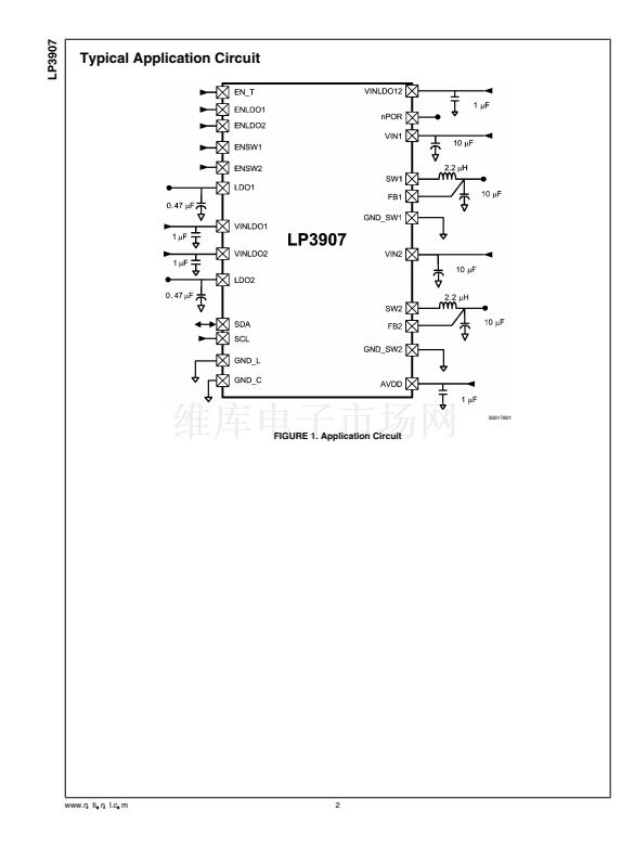
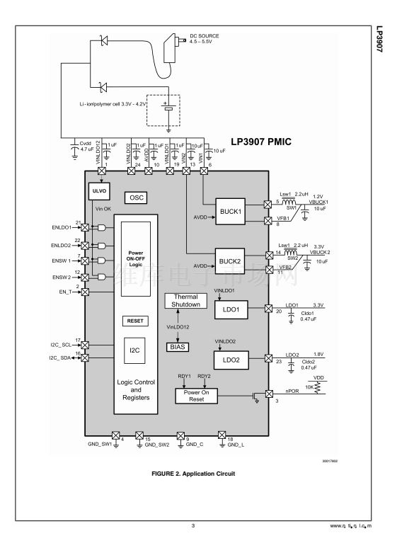
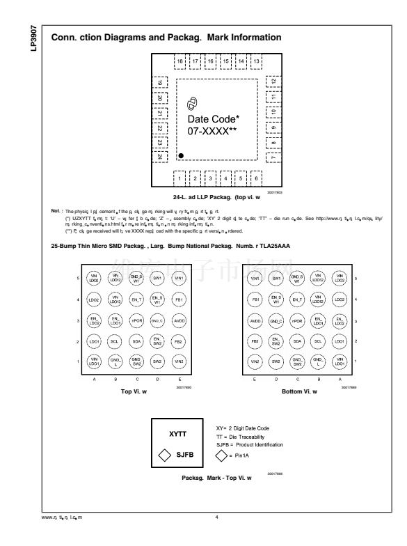
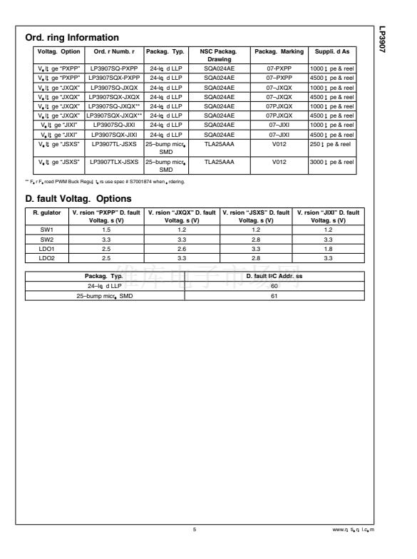
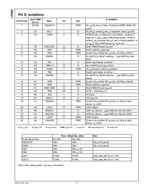
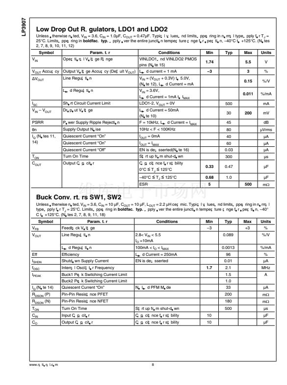
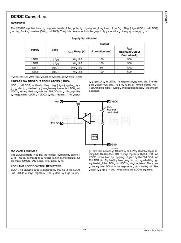
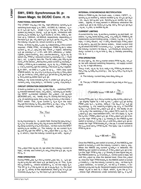
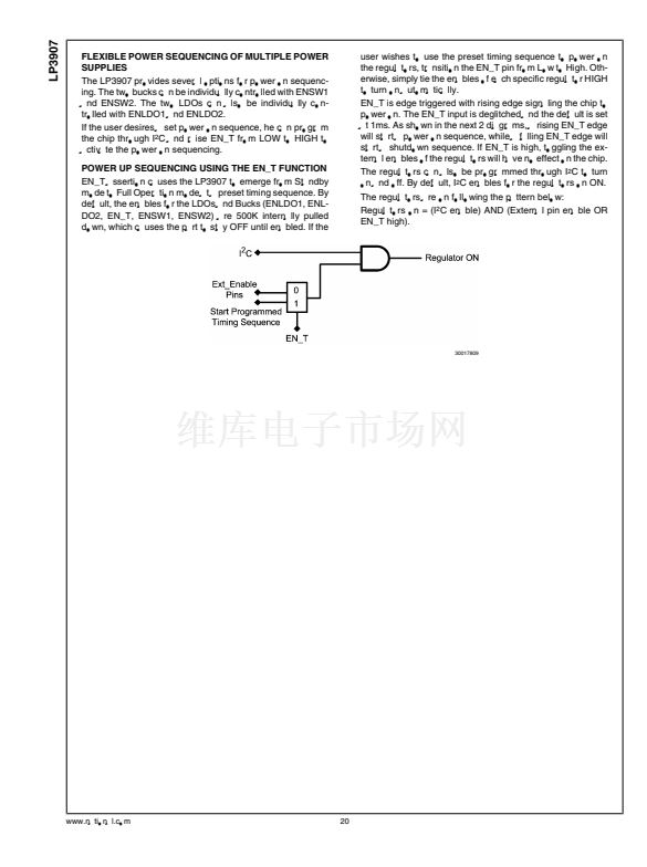
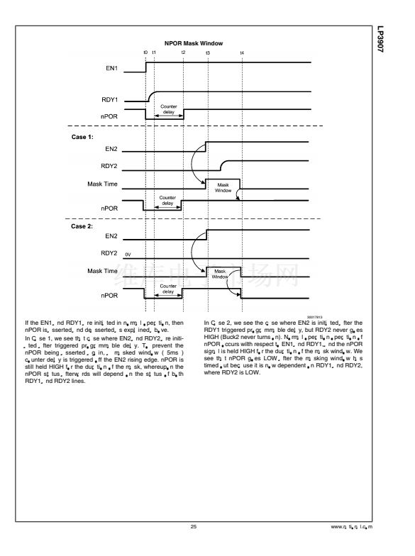
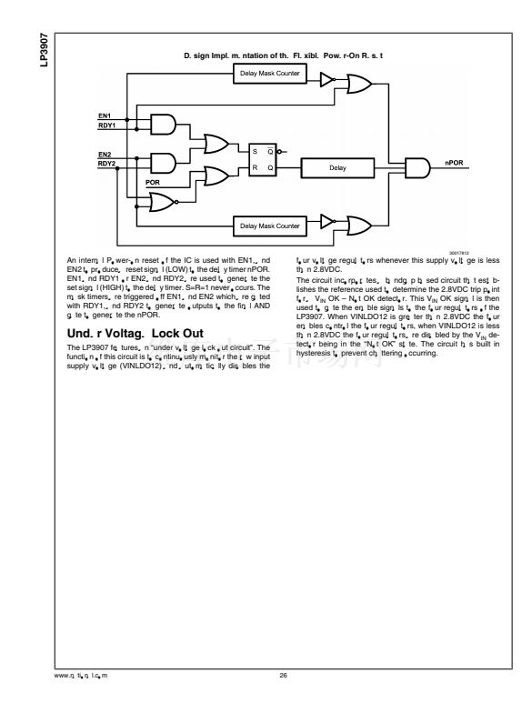
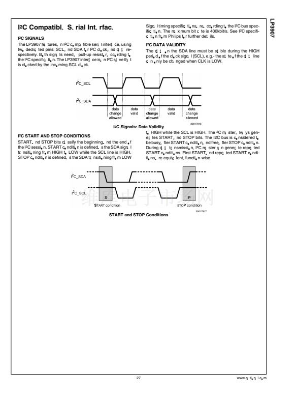
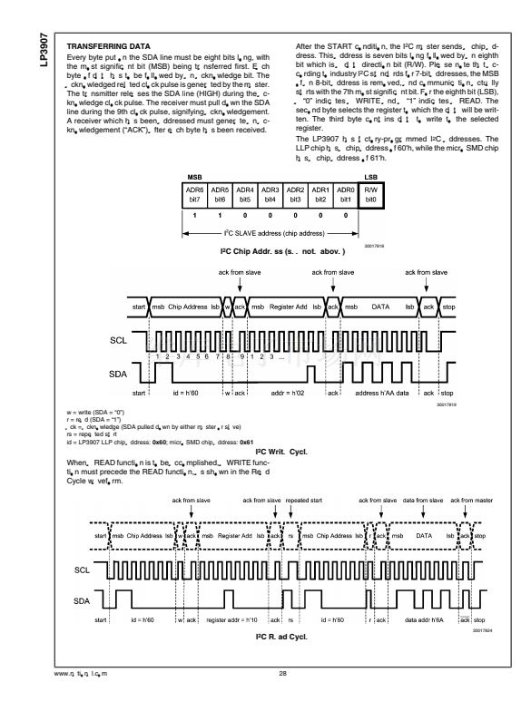
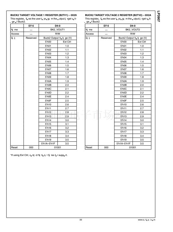
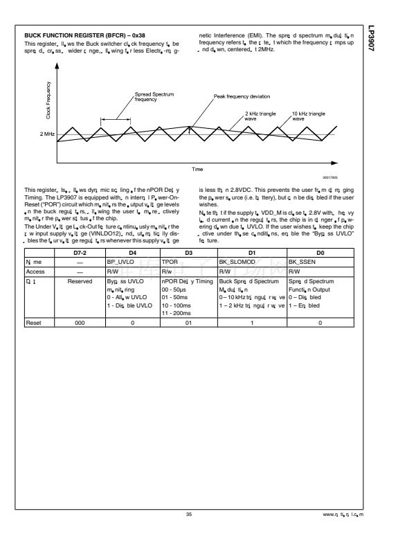
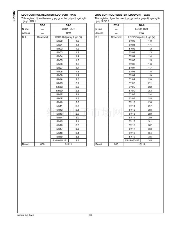
LP3907
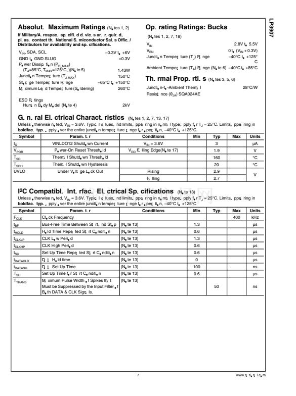
Absolute Maximum Ratings
(Notes 1, 2)
If Military/Aerospace specified devices are required,
please contact the National Semiconductor Sales Office/
Distributors for availability and specifications.
V
IN
, SDA, SCL
鈭?.3V to +6V
GND to GND SLUG
鹵0.3V
Power Dissipation (P
D_MAX
)
(T
A
=85擄C, T
MAX
=125擄C, )(Note 5)
1.43W
Junction Temperature (T
J-MAX
)
150擄C
Storage Temperature Range
鈭?5擄C to +150擄C
Maximum Lead Temperature (Soldering)
260擄C
ESD Ratings
Human Body Model (Note 4)
Operating Ratings: Bucks
(Notes 1, 2, 7, 18)
V
IN
V
EN
Junction Temperature (T
J
) Range
2.8V to 5.5V
0 to (V
IN
+ 0.3V)
鈭?0擄C to +125擄
C
Ambient Temperature (T
A
) Range (Note 6) 鈭?0擄C to +85擄C
Thermal Properties
Junction-to-Ambient Thermal
Resistance (胃
JA
) SQA024AE
(Notes 3, 5, 6)
28擄C/W
2kV
(Notes 1, 2, 7, 13, 17)
Unless otherwise noted, V
IN
= 3.6V. Typical values and limits appearing in normal type apply for T
J
= 25擄C. Limits appearing in
boldface type
apply over the entire junction temperature range for operation, 鈭?0擄C to +125擄C.
Symbol
I
Q
V
POR
T
SD
T
SDH
UVLO
Parameter
VINLDO12 Shutdown Current
Power-On Reset Threshold
Thermal Shutdown Threshold
Themal Shutdown Hysteresis
Under Voltage Lock Out
Rising
Falling
Conditions
V
IN
= 3.6V
V
DD
Falling Edge(Note 17)
Min
Typ
3
1.9
160
20
2.9
2.7
Max
Units
碌A(chǔ)
V
擄C
擄C
V
General Electrical Characteristics
(Note 13)
Unless otherwise noted, V
IN
= 3.6V. Typical values and limits appearing in normal type apply for T
J
= 25擄C. Limits appearing in
boldface type
apply over the entire junction temperature range for operation, 鈭?0擄C to +125擄C
Symbol
F
CLK
t
BF
t
HOLD
t
CLKLP
t
CLKHP
t
SU
t
DATAHLD
t
DATASU
T
SU
T
TRANS
Parameter
Clock Frequency
Bus-Free Time Between Start and Stop
Hold Time Repeated Start Condition
CLK Low Period
CLK High Period
Set Up Time Repeated Start Condition
Data Hold time
Data Set Up Time
Set Up Time for Start Condition
(Note 13)
(Note 13)
(Note 13)
(Note 13)
(Note 13)
(Note 13)
(Note 13)
(Note 13)
1.3
0.6
1.3
0.6
0.6
0
100
0.6
50
Conditions
Min
Typ
Max
400
Units
kHz
碌s
碌s
碌s
碌s
碌s
碌s
ns
碌s
ns
I
2
C Compatible Interface Electrical Specifications
Maximum Pulse Width of Spikes that
(Note 13)
Must be Suppressed by the Input Filter of
Both DATA & CLK Signals.
7
www.national.com


 1
1
 2
2
 3
3
 4
4
 5
5
 6
6
 7
7
 8
8
 9
9
 10
10
 11
11
 12
12
 13
13
 14
14
 15
15
 16
16
 17
17
 18
18
 19
19
 20
20
 21
21
 22
22
 23
23
 24
24
 25
25
 26
26
 27
27
 28
28
 29
29
 30
30
 31
31
 32
32
 33
33
 34
34
 35
35
 36
36
 37
37
 38
38
 39
39
 40
40
 41
41
 42
42
 43
43
 44
44
