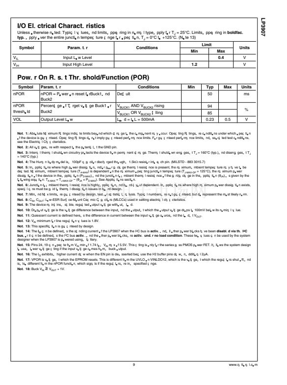
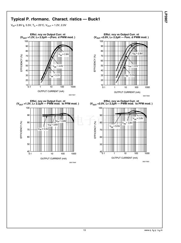
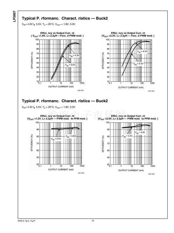
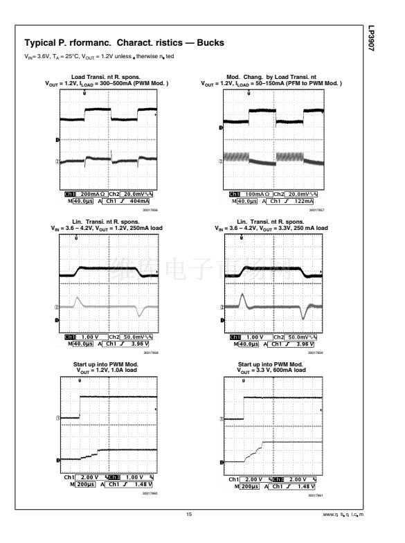
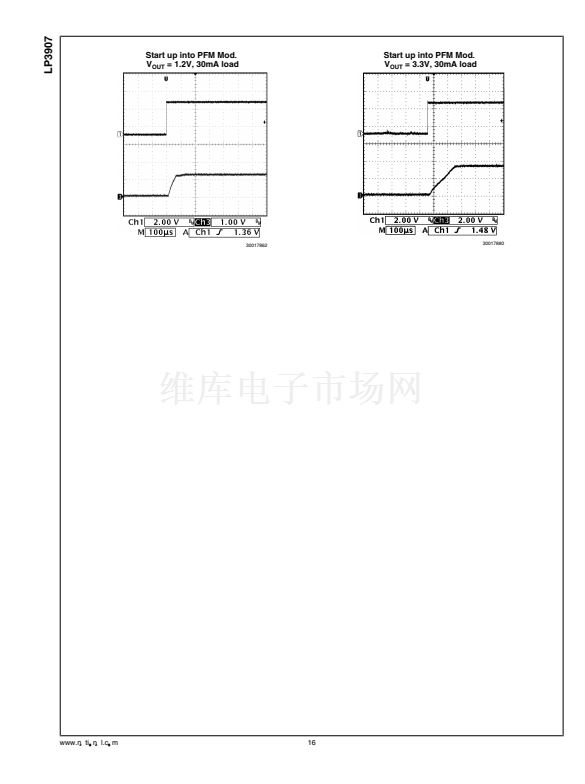
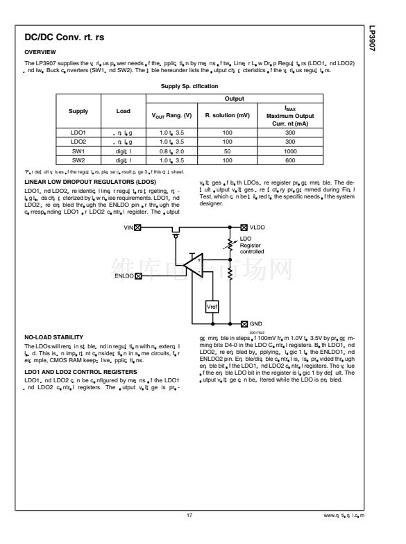
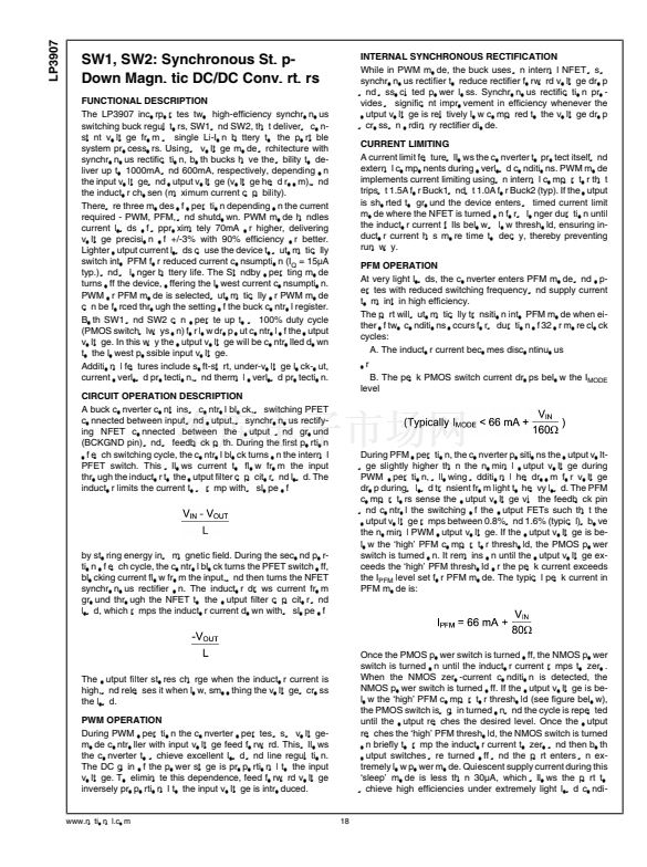
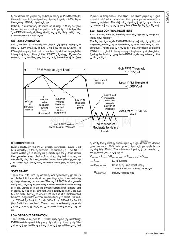
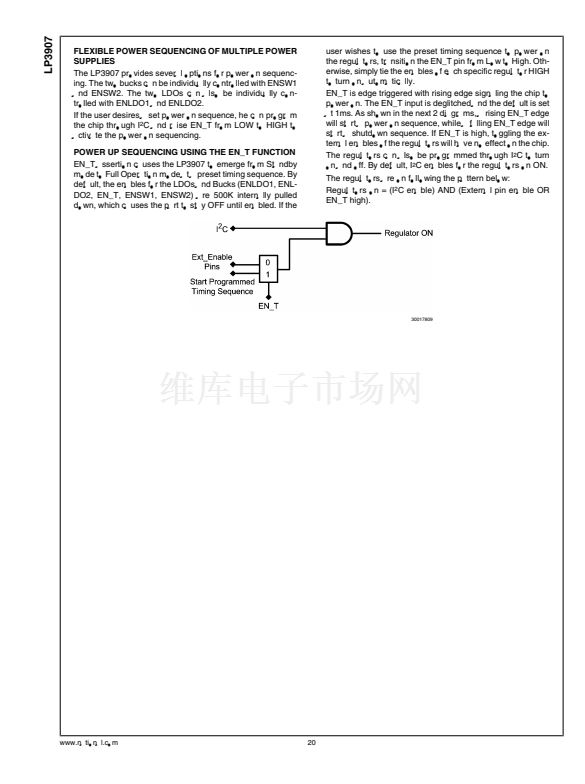
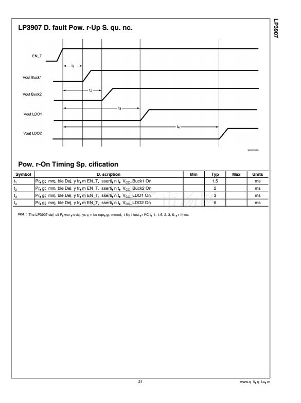
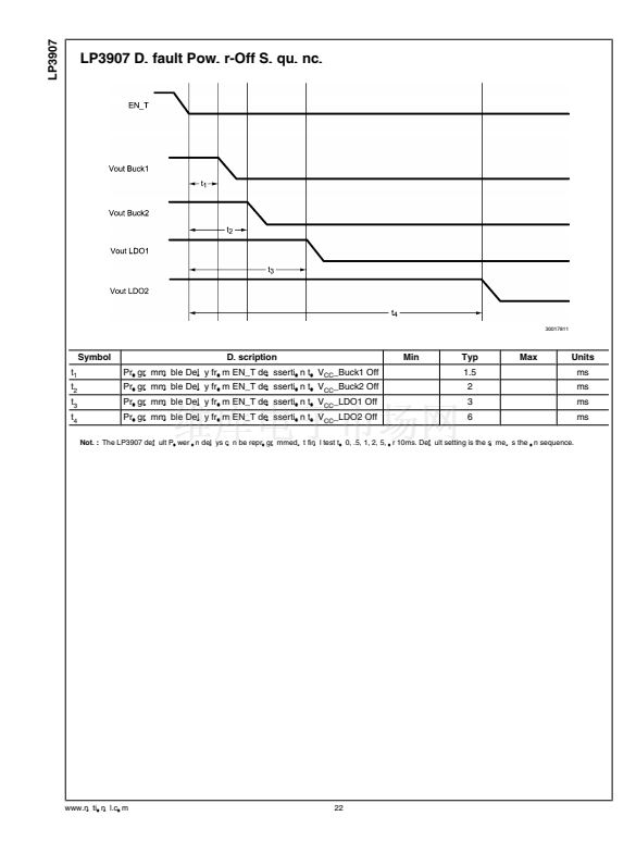
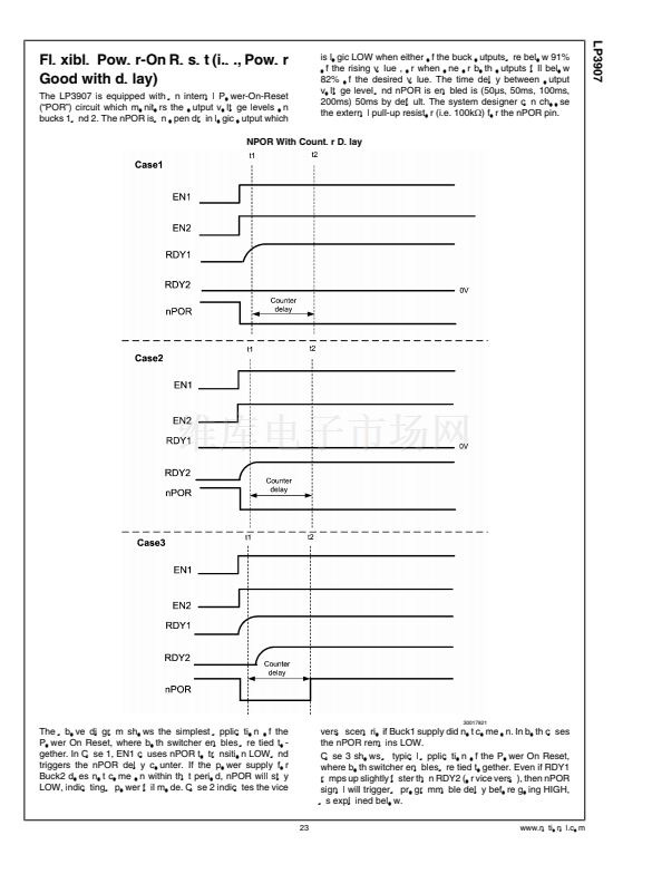
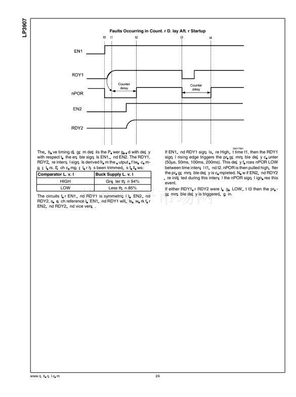
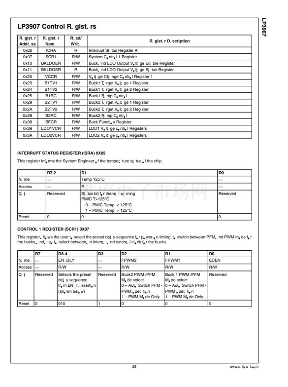
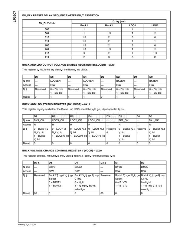
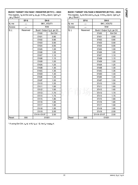
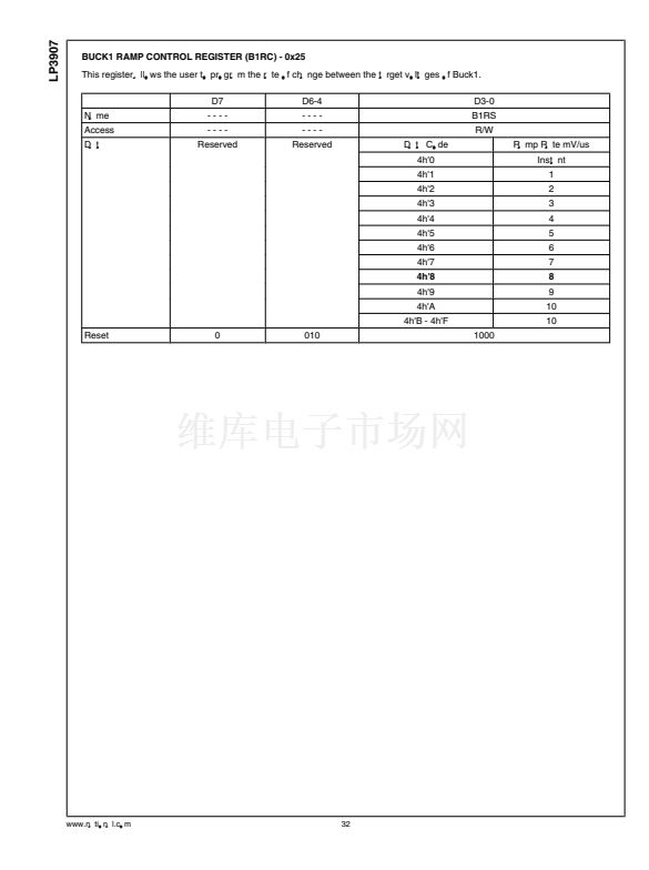
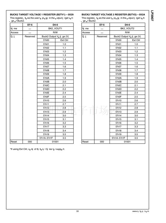
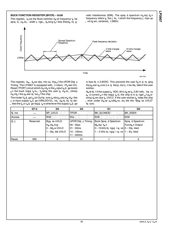
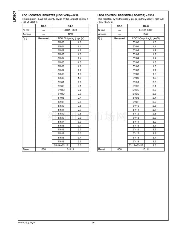
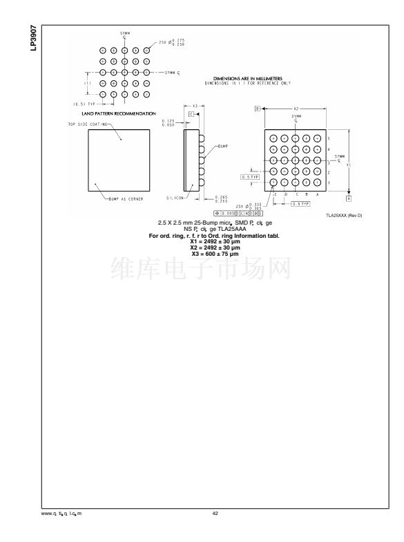
LP3907
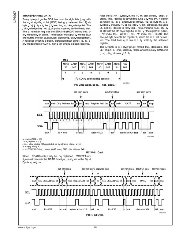
TRANSFERRING DATA
Every byte put on the SDA line must be eight bits long, with
the most significant bit (MSB) being transferred first. Each
byte of data has to be followed by an acknowledge bit. The
acknowledged related clock pulse is generated by the master.
The transmitter releases the SDA line (HIGH) during the ac-
knowledge clock pulse. The receiver must pull down the SDA
line during the 9th clock pulse, signifying acknowledgement.
A receiver which has been addressed must generate an ac-
knowledgement (鈥淎CK鈥? after each byte has been received.
After the START condition, the I
2
C master sends a chip ad-
dress. This address is seven bits long followed by an eighth
bit which is a data direction bit (R/W). Please note that ac-
cording to industry I
2
C standards for 7-bit addresses, the MSB
of an 8-bit address is removed, and communication actually
starts with the 7th most significant bit. For the eighth bit (LSB),
a 鈥?鈥?indicates a WRITE and a 鈥?鈥?indicates a READ. The
second byte selects the register to which the data will be writ-
ten. The third byte contains data to write to the selected
register.
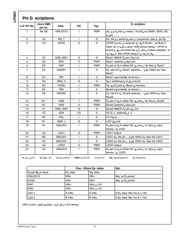
The LP3907 has factory-programmed I
2
C addresses. The
LLP chip has a chip address of 60'h, while the micro SMD chip
has a chip address of 61'h.
30017818
I
2
C Chip Address (see note above)
30017819
w = write (SDA = 鈥?鈥?
r = read (SDA = 鈥?鈥?
ack = acknowledge (SDA pulled down by either master or slave)
rs = repeated start
id = LP3907 LLP chip address:
0x60;
micro SMD chip address:
0x61
I
2
C Write Cycle
When a READ function is to be accomplished, a WRITE func-
tion must precede the READ function, as shown in the Read
Cycle waveform.
30017824
I
2
C Read Cycle
www.national.com
28


 1
1
 2
2
 3
3
 4
4
 5
5
 6
6
 7
7
 8
8
 9
9
 10
10
 11
11
 12
12
 13
13
 14
14
 15
15
 16
16
 17
17
 18
18
 19
19
 20
20
 21
21
 22
22
 23
23
 24
24
 25
25
 26
26
 27
27
 28
28
 29
29
 30
30
 31
31
 32
32
 33
33
 34
34
 35
35
 36
36
 37
37
 38
38
 39
39
 40
40
 41
41
 42
42
 43
43
 44
44
