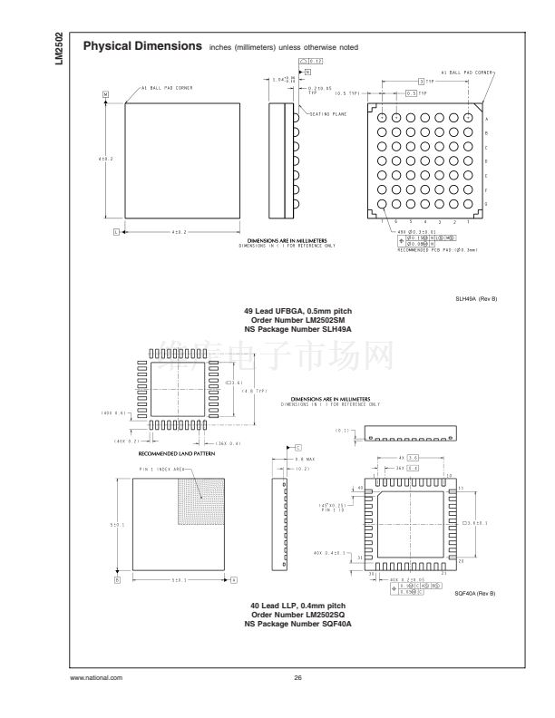
LM2502
Functional Description
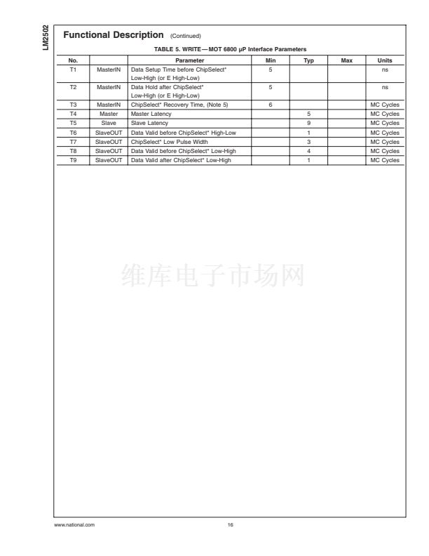
BUS OVERVIEW
The LM2502 is a dual link Transceiver configurable part that
supports a 16-bit CPU (m68 or i80) style interface. The MPL
physical layer is purpose-built for an extremely low power
and low EMI data transmission while requiring the fewest
number of signal lines. No external line components are
required, as termination is provided internal to the MPL
receiver. A maximum raw throughput of 307 Mbps (raw) is
possible with this chipset. When the protocol overhead is
taken into account, a maximum data throughput of 245 Mbps
is possible. The MPL interface is designed for use with
common 50鈩?to 100鈩?lines using standard materials and
connectors. Lines may be microstrip or stripline construction.
Total length of the interconnect is expected to be less than
20cm.
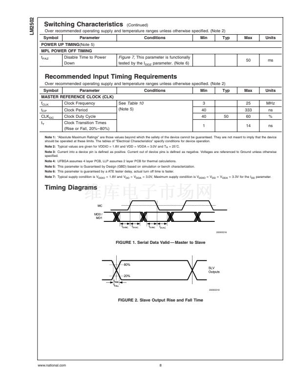
SERIAL BUS TIMING
Data valid is relative to both edges for a WRITE as shown in
Figure 4.
Data valid is specified as: Data Valid before Clock,
Data Valid after Clock, and Skew between data lines should
be less than 500ps.
20093303
FIGURE 4. Dual Link Timing (WRITE)
20093304
FIGURE 5. Dual Link Timing (READ)
Data is strobed out on the rising edge by the Slave for a
READ as shown in
Figure 5.
The Master monitors for the
start bit transition (Low to High) and selects the best strobe
to sample the incoming data on. This is done to account for
the round trip delay of the interconnect and application data
rate.
20093302
FIGURE 3. MPL Point-to-Point Bus
9
www.national.com


 1
1
 2
2
 3
3
 4
4
 5
5
 6
6
 7
7
 8
8
 9
9
 10
10
 11
11
 12
12
 13
13
 14
14
 15
15
 16
16
 17
17
 18
18
 19
19
 20
20
 21
21
 22
22
 23
23
 24
24
 25
25
 26
26
 27
27
