LM2502
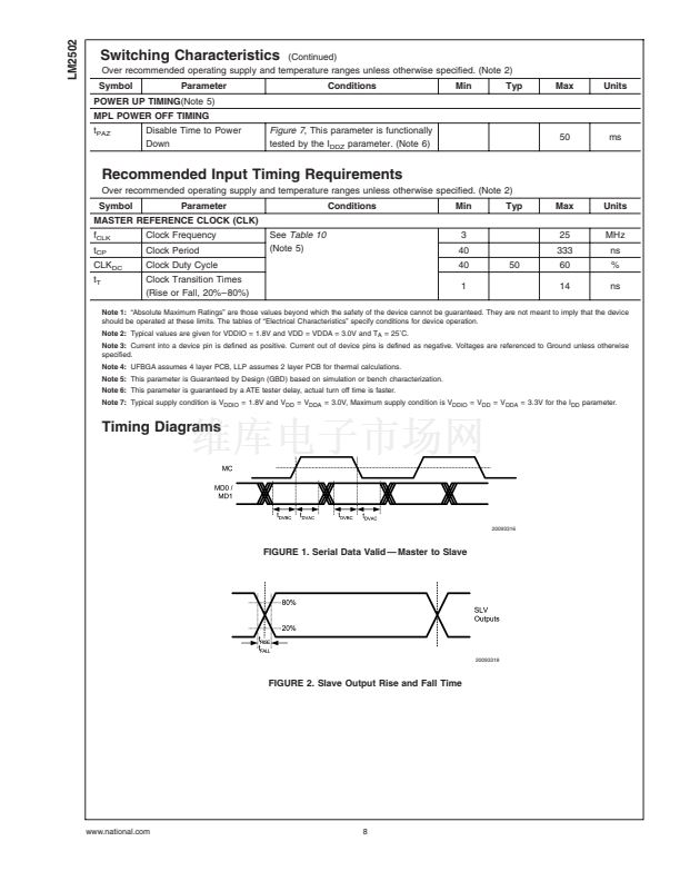
Switching Characteristics
Symbol
Parameter
POWER UP TIMING(Note
5)
MPL POWER OFF TIMING
t
PAZ
Disable Time to Power
Down
(Continued)
Over recommended operating supply and temperature ranges unless otherwise specified. (Note 2)
Conditions
Min
Typ
Max
Units
Figure 7,
This parameter is functionally
tested by the I
DDZ
parameter. (Note 6)
50
ms
Recommended Input Timing Requirements
Over recommended operating supply and temperature ranges unless otherwise specified. (Note 2)
Symbol
f
CLK
t
CP
CLK
DC
t
T
Parameter
Clock Frequency
Clock Period
Clock Duty Cycle
Clock Transition Times
(Rise or Fall, 20%鈥?0%)
See
Table 10
(Note 5)
Conditions
Min
3
40
40
1
50
Typ
Max
25
333
60
14
Units
MHz
ns
%
ns
MASTER REFERENCE CLOCK (CLK)
Note 1:
鈥淎bsolute Maximum Ratings鈥?are those values beyond which the safety of the device cannot be guaranteed. They are not meant to imply that the device
should be operated at these limits. The tables of 鈥淓lectrical Characteristics鈥?specify conditions for device operation.
Note 2:
Typical values are given for VDDIO = 1.8V and VDD = VDDA = 3.0V and T
A
= 25藲C.
Note 3:
Current into a device pin is defined as positive. Current out of device pins is defined as negative. Voltages are referenced to Ground unless otherwise
specified.
Note 4:
UFBGA assumes 4 layer PCB, LLP assumes 2 layer PCB for thermal calculations.
Note 5:
This parameter is Guaranteed by Design (GBD) based on simulation or bench characterization.
Note 6:
This parameter is guaranteed by a ATE tester delay, actual turn off time is faster.
Note 7:
Typical supply condition is V
DDIO
= 1.8V and V
DD
= V
DDA
= 3.0V, Maximum supply condition is V
DDIO
= V
DD
= V
DDA
= 3.3V for the I
DD
parameter.
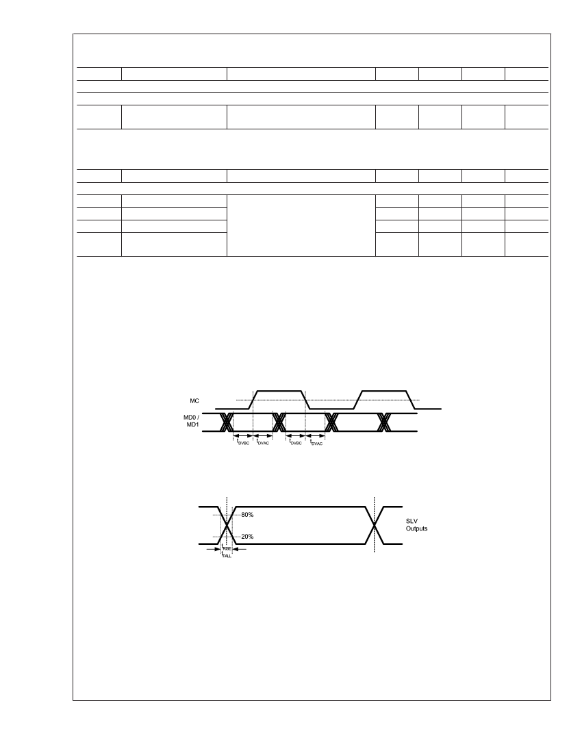
Timing Diagrams
20093316
FIGURE 1. Serial Data Valid 鈥?Master to Slave
20093318
FIGURE 2. Slave Output Rise and Fall Time
www.national.com
8


 1
1
 2
2
 3
3
 4
4
 5
5
 6
6
 7
7
 8
8
 9
9
 10
10
 11
11
 12
12
 13
13
 14
14
 15
15
 16
16
 17
17
 18
18
 19
19
 20
20
 21
21
 22
22
 23
23
 24
24
 25
25
 26
26
 27
27
