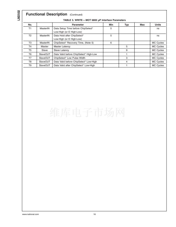
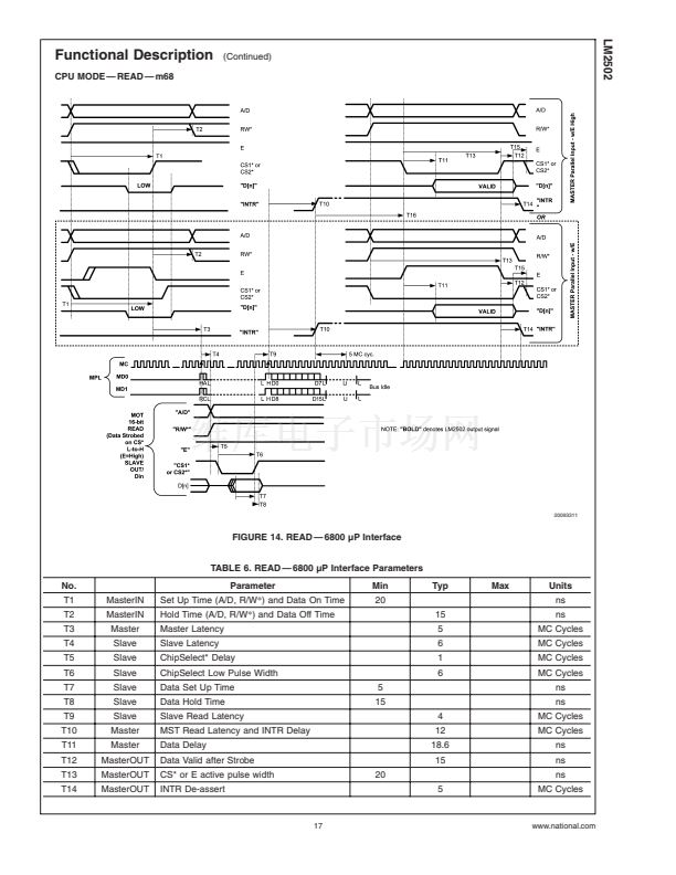
LM2502
Electrical Characteristics
Symbol
I
DD
Parameter
Total Supply
Current 鈥?Enabled
Conditions: MC = 76.8
MHz, MD = 1010-0101
pattern (worse case toggle,
rail-to-rail levels), CLK =
19.2 MHz (4X) (Note 7)
Total Supply
Current 鈥?Enabled
Conditions: MC = 20 MHz,
MD = 1010-0101 pattern
(worse case toggle,
rail-to-rail levels), CLK = 5
MHz (4X)
I
DDZ
Supply Current 鈥?Disabled
SUPPLY CURRENT
(Continued)
Over recommended operating supply and temperature ranges unless otherwise specified. (Notes 2, 3)
Conditions
Master
V
DDIO
V
DD
= V
DDA
Slave, C
L
= 10 pF
V
DDIO
V
DD
= V
DDA
Master
V
DDIO
= 1.8V
V
DD
= V
DDA
= 3V
Slave, C
L
= 10 pF
V
DDIO
= 1.8V
V
DD
= V
DDA
= 3V
Power_Down Mode, PD* = 0V
Min
Typ
Max
Units
15
14
1.5
9.0
10
5
1
4
1
220
25
9.0
13.0
碌A(chǔ)
mA
mA
mA
碌A(chǔ)
mA
mA
mA
10
碌A(chǔ)
Switching Characteristics
Over recommended operating supply and temperature ranges unless otherwise specified. (Note 2)
Symbol
t
SET
t
HOLD
t
RISE
Parameter
Set Up Time, Data to Edge
Hold Time, Edge to Data
Rise Time
Figure 2,
Outputs,
C
L
= 10 pF
Edge sensitive
outputs tested
only:
m68 mode: CS1
*
,
CS2
*
and CLKout
i80 mode: RD
*
,
WR
*
, and CLKout
V
DDIO
= 1.7V
V
DDIO
= 3.3V
V
DDIO
= 1.7V
V
DDIO
= 3.3V
Inputs
Conditions
Min
5
5
2
1
2
1
7
2
6
2
50
14
10
14
10
Typ
Max
Units
ns
ns
ns
ns
ns
ns
%
PARALLEL BUS TIMING
t
FALL
Fall Time
CLK
DC
Output Clock Duty Cycle
CLKDIS
*
= H, Slave (DES)
Parallel Bus Timing
- See
Figures 13, 14, 15, 16
and
Table 5, Table 6, Table 7,
and
Table 8
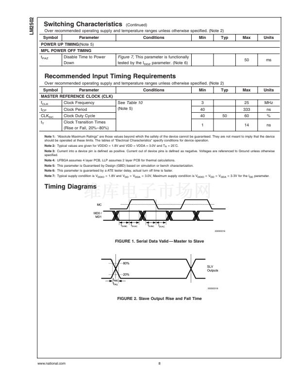
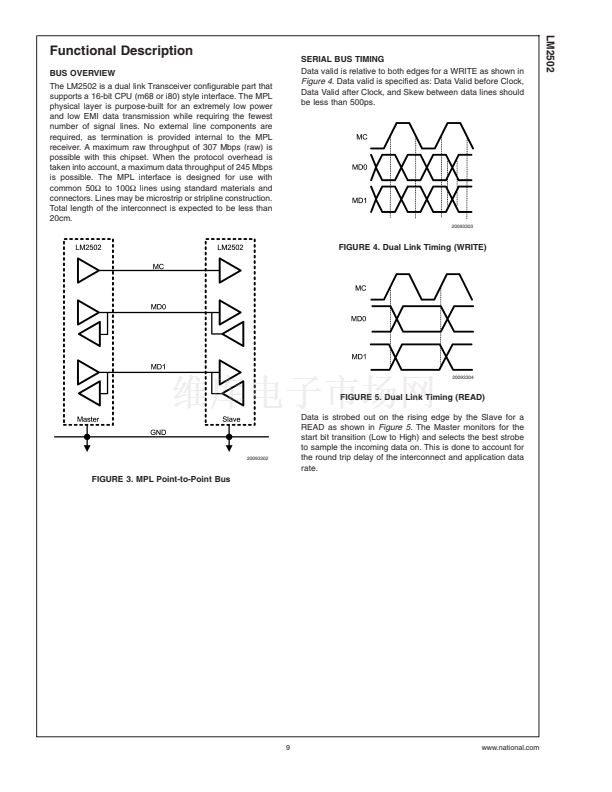
SERIAL BUS TIMING
t
DVBC
t
DVAC
t
0
t
1
t
2
t
3
t
4
t
5
Data Valid before Clock
Data Valid after Clock
Master PLL Lock Counter
MC Pulse Width Low
(Master)
MC Pulse Width HIGH
(Master)
MC Pulse Width Low
(Master)
CLK-Out Delay (Slave)
Power Up Total delay
(t
0
+ t
1
+ t
2
+ t
3
+ t
4
)
7
Master-to-Slave
(Note 5)
Figure 6
2.0
0.5
ns
ns
CLK
cycles
CLK
cycles
CLK
cycles
CLK
cycles
MC
cycles
CLK
cycles
www.national.com
POWER UP TIMING(Note
5)
4096
11
11
11
7
4133


 1
1
 2
2
 3
3
 4
4
 5
5
 6
6
 7
7
 8
8
 9
9
 10
10
 11
11
 12
12
 13
13
 14
14
 15
15
 16
16
 17
17
 18
18
 19
19
 20
20
 21
21
 22
22
 23
23
 24
24
 25
25
 26
26
 27
27
