Theory of Operation
The LM2408 is a high voltage monolithic triple CRT driver
suitable for SVGA and XGA display applications The
LM2408 features
a
80V operation and low power dissipa-
tion The part is housed in the industry standard 11-Lead
TO-220 molded plastic power package
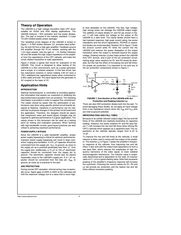
The simplified circuit diagram of the LM2408 is shown in
Figure 1
A PNP emitter follower Q1 provides input buffer-
ing Q2 and Q3 form a high gain amplifier Feedback around
this amplifier through the 15 kX resistor working with the
1 kX input resistor sets the gain to
b
15 Emitter followers
Q5 and Q6 isolate the high output impedance of the amplifi-
er from the capacitance of the CRT cathode and make the
circuit relative insensitive to load capacitance
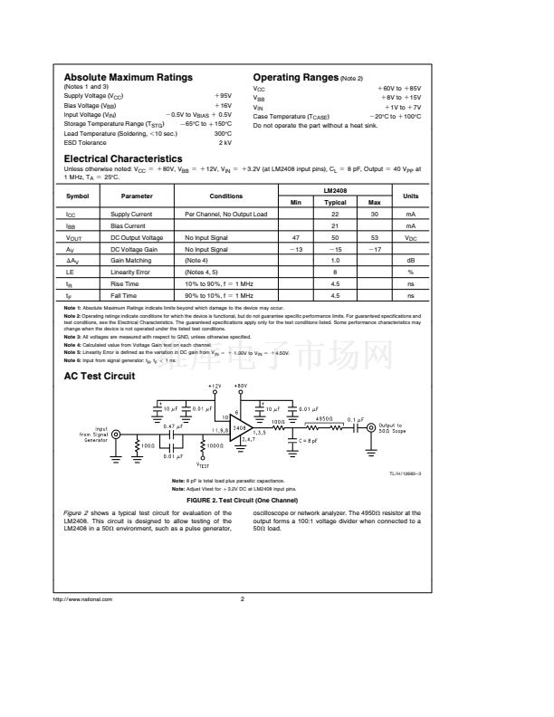
Figure 2
shows a typical test circuit for evaluation of the
LM2408 This circuit is designed to allow testing of the
LM2408 in a 50X environment such as a pulse generator
and a scope or a network analyzer In this test circuit two
low inductance resistors in series totaling 4 95 kX form a
100 1 wideband low capacitance probe when connected to
a 50X cable and load The input signal from the generator is
AC coupled to the base of Q1
er than allowable on the LM2408 This fast high voltage
high energy pulse can damage the LM2408 output stage
The addition of clamp diodes D1 and D2 (as shown in
Fig-
ure 7
) will help clamp the voltage at the output of the
LM2408 to a safe level The clamp diodes should have a
fast transient response high peak current rating low series
impedance and low shunt capacitance FDH400 or equiva-
lent diodes are recommended Resistor R2 in
Figure 7
limits
the arcover current while R1 limits the current into the
LM2408 and reduces the power dissipation of the output
transistors when the output is stressed beyond the supply
voltage Peaking inductor Lp also helps protect the LM2408
from CRT arcover and is part of the arc protection circuit
Having large value resistors for R1 and R2 would be desir-
able but this has the effect of increasing rise and fall times
For proper arc protection it is important to not omit any of
the arc protection components shown in
Figure 7
Application Hints
INTRODUCTION
National Semiconductor is committed to providing applica-
tion information that assists our customers in obtaining the
best performance possible from our products The following
information is provided in order to support this commitment
The reader should be aware that the optimization of per-
formance was done using specific printed circuit boards de-
signed at National Variations in performance can be real-
ized due to physical changes in the printed circuit board and
the application Therefore the designer should be aware
that component value and board layout changes may be
required to optimize performance in a given application The
values shown in this document can be used as a staring
point for testing and evaluation purposes When working
with high bandwidth circuits good layout practices are also
critical to achieving maximum performance
POWER SUPPLY BYPASS
Since the LM2408 is a wide bandwidth amplifier proper
power supply bypassing is critical for optimum performance
Improper power supply bypassing can result in large over-
shoot ringing and oscillation A 0 01
mF
capacitor should be
connected from the supply pin V
CC
to ground as close to
the supply pin as is practical (preferably less than
from
the supply pin) Additionally a 10
mF
to 100
mF
electrolytic
capacitor should be connected from the supply pin to
ground The electrolytic capacitor should also be placed
reasonably close to the LM2408鈥檚 supply pin A 0 1
mF
ca-
pacitor should be connected from the bias pin V
BB
to
ground as close as is practical to the part
ARC PROTECTION
During normal CRT operation internal arcing may occasion-
ally occur Spark gaps of 200V to 300V at the cathodes will
limit the maximum voltage but to a value that is much high-
TL H 12683 鈥?8
FIGURE 7 One Section of the LM2408 with Arc
Protection and Peaking Inductor L
P
There are also ESD protection diodes built into the part To
avoid damaging these diodes do not apply an input voltage
from a low impedance source when the V
BB
and V
CC
pins
are held at ground potential
IMPROVING RISE AND FALL TIMES
Because of an emitter follower output stage the rise and fall
times of the LM2408 are relatively insensitive to capactive
loading However the series resistors R1 and R2 (see
Fig-
ure 7
) will increase the rise and fall times when driving the
CRT鈥檚 cathode which appears as a capacitive load The ca-
pacitance at the cathode typically ranges from 8 pF to
12 pF
To improve the rise and fall times at the cathode a small
inductor is often used in series with the output of the amplifi-
er The inductor L
P
in
Figure 7
peaks the amplifier鈥檚 frequen-
cy response at the cathode thus improving rise and fall
times It also acts with the output load capacitance to form a
low pass filter which reduces the amplitudes of high fre-
quency harmonics of the video signal to lower radiated
electromagnetic interference The inductor value is empiri-
cally determined and is dependent on the load An inductor
value of 0 1
mH
is a good starting value Note that excessive
peaking of the amplifier鈥檚 frequency response will increase
the overshoot Choosing the correct values for R1 R2 and
Lp will provide arc protection and the fastest rise and fall
times without excessive peaking
http
www national com
4


 1
1
 2
2
 3
3
 4
4
 5
5
 6
6
 7
7
 8
8
