Absolute Maximum Ratings
(Notes 1 and 3)
Supply Voltage (V
CC
)
Bias Voltage (V
BB
)
Input Voltage (V
IN
)
a
95V
a
16V
Operating Ranges
(Note 2)
V
CC
V
BB
V
IN
Case Temperature (T
CASE
)
Do not operate the part without a heat sink
a
60V to
a
85V
a
8V to
a
15V
a
1V to
a
7V
b
20 C to
a
100 C
b
0 5V to V
BIAS
a
0 5V
b
65 C to
a
150 C
Storage Temperature Range (T
STG
)
Lead Temperature (Soldering
k
10 sec )
ESD Tolerance
300 C
2 kV
Electrical Characteristics
Unless otherwise noted V
CC
e a
80V V
BB
e a
12V V
IN
e a
3 2V (at LM2408 input pins) C
L
e
8 pF Output
e
40 V
PP
at
1 MHz T
A
e
25 C
Symbol
I
CC
I
BB
V
OUT
A
V
DA
V
LE
t
R
t
F
Parameter
Supply Current
Bias Current
DC Output Voltage
DC Voltage Gain
Gain Matching
Linearity Error
Rise Time
Fall Time
No Input Signal
No Input Signal
(Note 4)
(Notes 4 5)
10% to 90% f
e
1 MHz
90% to 10% f
e
1 MHz
47
b
13
Conditions
Min
Per Channel No Output Load
LM2408
Typical
22
21
50
b
15
Units
Max
30
mA
mA
53
b
17
V
DC
10
8
45
45
dB
%
ns
ns
Note 1
Absolute Maximum Ratings indicate limits beyond which damage to the device may occur
Note 2
Operating ratings indicate conditions for which the device is functional but do not guarantee specific performance limits For guaranteed specifications and
test conditions see the Electrical Characteristics The guaranteed specifications apply only for the test conditions listed Some performance characteristics may
change when the device is not operated under the listed test conditions
Note 3
All voltages are measured with respect to GND unless otherwise specified
Note 4
Calculated value from Voltage Gain test on each channel
Note 5
Linearity Error is defined as the variation in DC gain from V
IN
e a
1 90V to V
IN
e a
4 50V
Note 6
Input from signal generator t
R
t
F
k
1 ns
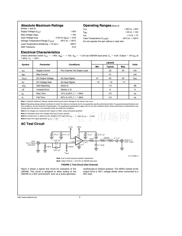
AC Test Circuit
TL H 12683 鈥?3
Note
8 pF is total load plus parasitic capacitance
Note
Adjust Vtest for
a
3 2V DC at LM2408 input pins
FIGURE 2 Test Circuit (One Channel)
Figure 2
shows a typical test circuit for evaluation of the
LM2408 This circuit is designed to allow testing of the
LM2408 in a 50X environment such as a pulse generator
oscilloscope or network analyzer The 4950X resistor at the
output forms a 100 1 voltage divider when connected to a
50X load
http
www national com
2


 1
1
 2
2
 3
3
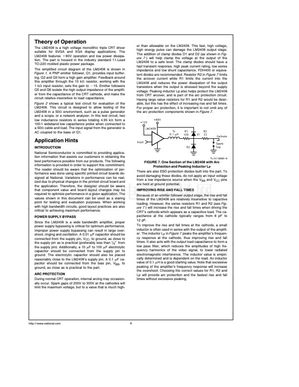 4
4
 5
5
 6
6
 7
7
 8
8
