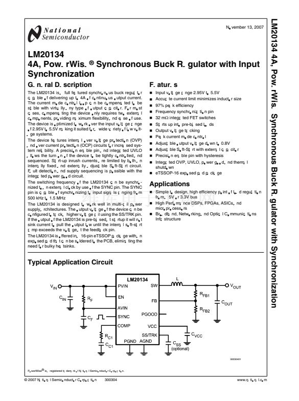
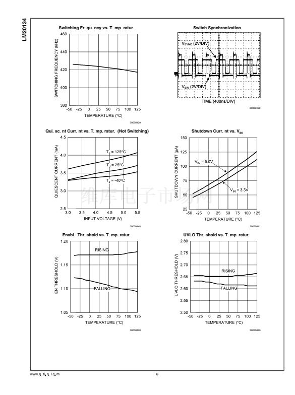
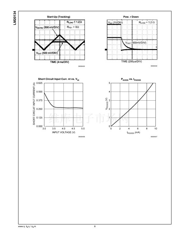
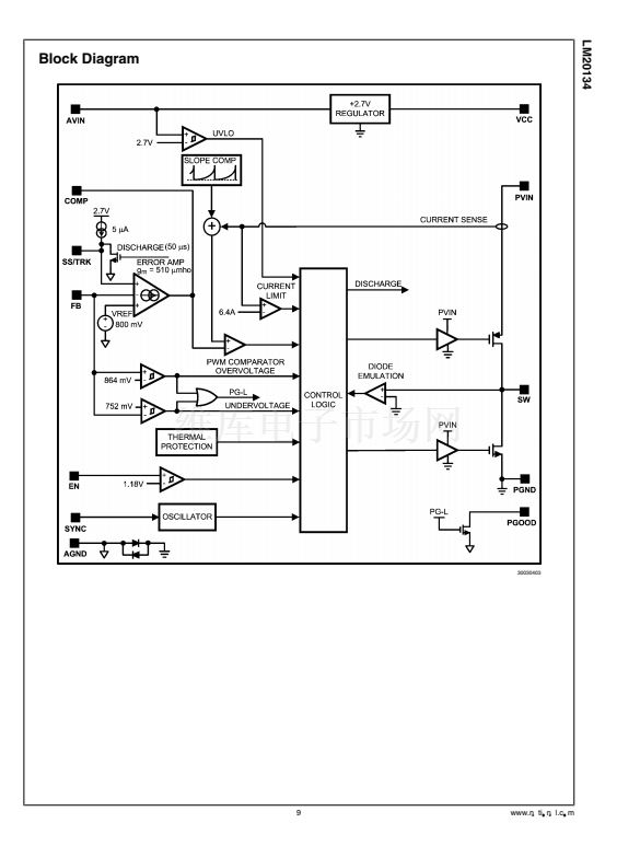
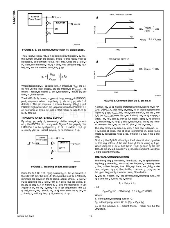
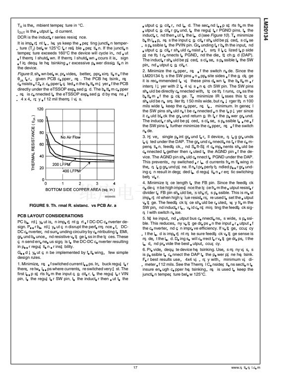
LM20134
Where, C
OUT
(F) is the minimum required output capacitance,
L (H) is the value of the inductor, V
DROOP
(V) is the output
voltage drop ignoring loop bandwidth considerations,
螖I
OUT-
STEP
(A) is the load step change, R
ESR
(鈩?
is the output
capacitor ESR, V
IN
(V) is the input voltage, and V
OUT
(V) is
the set regulator output voltage. Both the tolerance and volt-
age coefficient of the capacitor needs to be examined when
designing for a specific output ripple or transient drop target.
INPUT CAPACITOR SELECTION (C
IN
)
Good quality input capacitors are necessary to limit the ripple
voltage at the VIN pin while supplying most of the switch cur-
rent during the on-time. In general it is recommended to use
a ceramic capacitor for the input as they provide both a low
impedance and small footprint. One important note is to use
a good dielectric for the ceramic capacitor such as X5R or
X7R. These provide better over temperature performance
and also minimize the DC voltage derating that occurs on Y5V
capacitors. For most applications, a 22 碌F, X5R, 6.3V input
capacitor is sufficient; however, additional capacitance may
be required if the connection to the input supply is far from the
PVIN pins. The input capacitor should be placed as close as
possible PVIN and PGND pins of the device.
Non-ceramic input capacitors should be selected for RMS
current rating and minimum ripple voltage. A good approxi-
mation for the required ripple current rating is given by the
relationship:
capacitor, inductor, load, and the device itself.
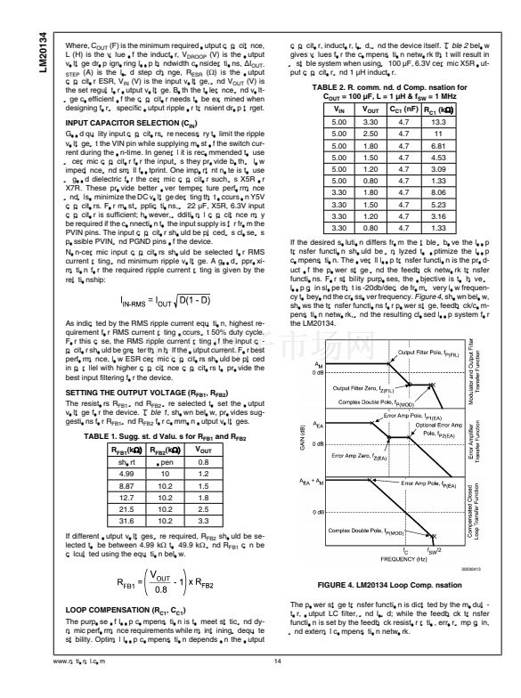
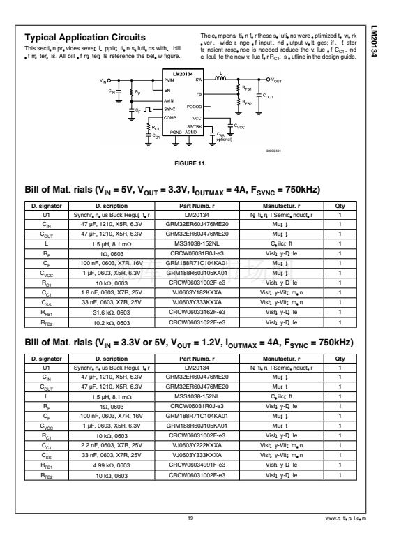
Table 2
below
gives values for the compensation network that will result in
a stable system when using a 100 碌F, 6.3V ceramic X5R out-
put capacitor and 1 碌H inductor.
TABLE 2. Recommended Compensation for
C
OUT
= 100 碌F, L = 1 碌H & f
SW
= 1 MHz
V
IN
5.00
5.00
5.00
5.00
5.00
5.00
3.30
3.30
3.30
3.30
V
OUT
3.30
2.50
1.80
1.50
1.20
0.80
1.80
1.50
1.20
0.80
C
C1
(nF) R
C1
(k鈩?
4.7
4.7
4.7
4.7
4.7
4.7
4.7
4.7
4.7
4.7
13.3
11
6.81
4.53
3.09
1.33
8.06
5.23
3.16
1.33
As indicated by the RMS ripple current equation, highest re-
quirement for RMS current rating occurs at 50% duty cycle.
For this case, the RMS ripple current rating of the input ca-
pacitor should be greater than half the output current. For best
performance, low ESR ceramic capacitors should be placed
in parallel with higher capacitance capacitors to provide the
best input filtering for the device.
SETTING THE OUTPUT VOLTAGE (R
FB1
, R
FB2
)
The resistors R
FB1
and R
FB2
are selected to set the output
voltage for the device.
Table 1,
shown below, provides sug-
gestions for R
FB1
and R
FB2
for common output voltages.
TABLE 1. Suggested Values for R
FB1
and R
FB2
R
FB1
(k鈩?
short
4.99
8.87
12.7
21.5
31.6
R
FB2
(k鈩?
open
10
10.2
10.2
10.2
10.2
V
OUT
0.8
1.2
1.5
1.8
2.5
3.3
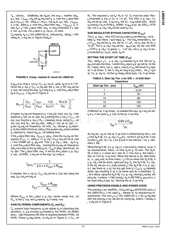
If the desired solution differs from the table above the loop
transfer function should be analyzed to optimize the loop
compensation. The overall loop transfer function is the prod-
uct of the power stage and the feedback network transfer
functions. For stability purposes, the objective is to have a
loop gain slope that is -20db/decade from a very low frequen-
cy to beyond the crossover frequency.
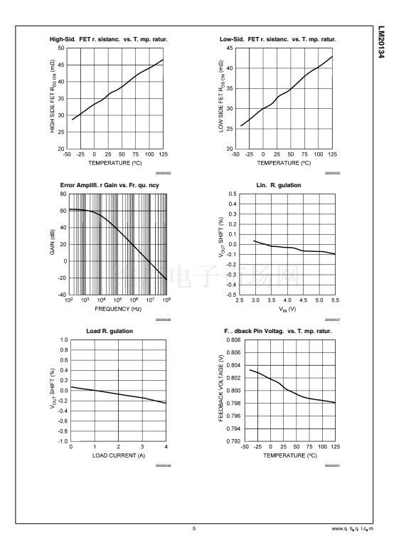
Figure 4,
shown below,
shows the transfer functions for power stage, feedback/com-
pensation network, and the resulting closed loop system for
the LM20134.
If different output voltages are required, R
FB2
should be se-
lected to be between 4.99 k鈩?to 49.9 k鈩?and R
FB1
can be
calculated using the equation below.
30030413
FIGURE 4. LM20134 Loop Compensation
LOOP COMPENSATION (R
C1
, C
C1
)
The purpose of loop compensation is to meet static and dy-
namic performance requirements while maintaining adequate
stability. Optimal loop compensation depends on the output
www.national.com
14
The power stage transfer function is dictated by the modula-
tor, output LC filter, and load; while the feedback transfer
function is set by the feedback resistor ratio, error amp gain,
and external compensation network.


 1
1
 2
2
 3
3
 4
4
 5
5
 6
6
 7
7
 8
8
 9
9
 10
10
 11
11
 12
12
 13
13
 14
14
 15
15
 16
16
 17
17
 18
18
 19
19
 20
20
 21
21
 22
22
