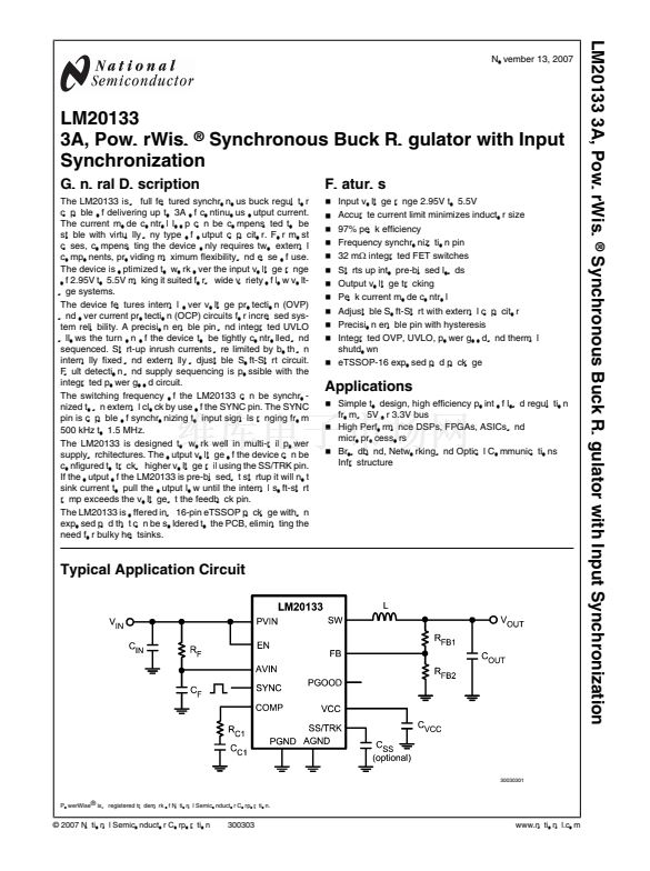
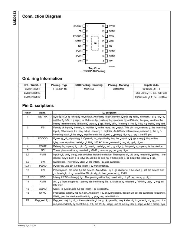
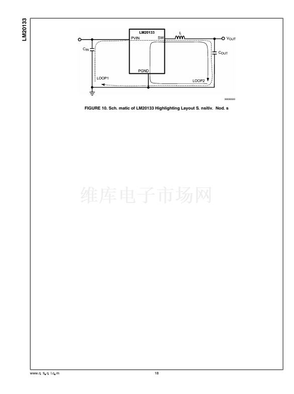
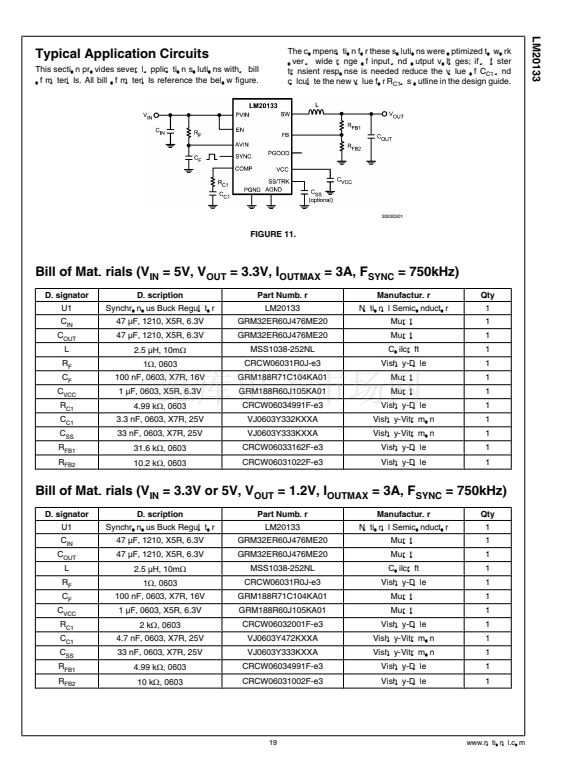
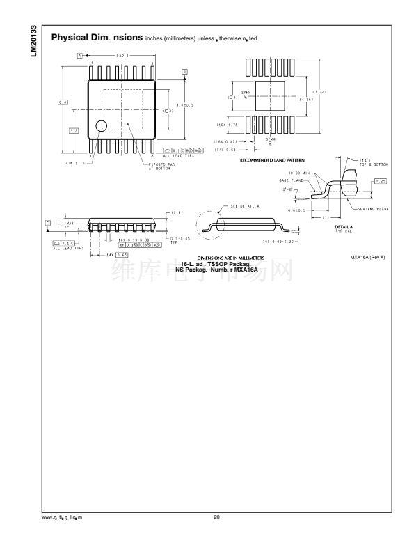
LM20133
Absolute Maximum Ratings
(Note 1)
If Military/Aerospace specified devices are required,
please contact the National Semiconductor Sales Office/
Distributors for availability and specifications.
Voltages from the indicated pins to GND
AVIN, PVIN, EN, PGOOD, SS/
TRK, COMP, FB, SW, SYNC
Storage Temperature
Junction Temperature
-0.3V to +6V
-65擄C to 150擄C
150擄C
Power Dissipation (Note 2)
Lead Temperature (Soldering,
10 sec)
Minimum ESD Rating (Note 3)
2.6W
260擄C
鹵2kV
Operating Ratings
PVIN, AVIN to GND
Junction Temperature
2.95V to 5.5V
鈭?0擄C to + 125擄C
Electrical Characteristics
Unless otherwise stated, the following conditions apply: AVIN = PVIN = VIN = 5V.
Limits in standard type are for T
J
= 25擄C only, limits in bold face type apply over the junction temperature (T
J
) range of -40擄C to
+125擄C. Minimum and Maximum limits are guaranteed through test, design, or statistical correlation. Typical values represent the
most likely parametric norm at T
J
= 25擄C, and are provided for reference purposes only.
Symbol
V
FB
螖V
OUT
/螖I
OUT
I
CL
R
DS_ON
R
DS_ON
I
Q
I
SD
V
UVLO
V
UVLO_HYS
V
VCC
I
SS
V
TRACK
Oscillator
F
OSC
F
OSCH
F
OSCL
V
IH_SYNC
V
IL_SYNC
I
SYNC
T
OFF_TIME
T
ON_TIME
T
CL_BLANK
I
FB
I
COMP_SRC
I
COMP_SNK
g
m
A
VOL
Power Good
V
OVP
V
OVP_HYS
V
PGTH
V
PGHYS
T
PGOOD
I
OL
I
OH
Over Voltage Protection Rising Threshold
Over Voltage Protection Hysteresis
PGOOD Rising Threshold
PGOOD Falling Hysteresis
PGOOD deglitch time
PGOOD Low Sink Current
PGOOD High Leakage Current
V
PGOOD
= 0.4V
V
PGOOD
= 5V
3
Parameter
Feedback pin voltage
Load Regulation
Switch Current Limit Threshold
High-Side Switch On Resistance
Low-Side Switch On Resistance
Operating Quiescent Current
Shutdown Quiescent current
VIN Under Voltage Lockout
VIN Under Voltage Lockout Hysteresis
VCC Voltage
Soft-Start Pin Source Current
SS/TRK Accuracy, V
SS
- V
FB
Oscillator Frequency
Maximum External SYNC Frequency
Minimum External SYNC Frequency
SYNC pin Logic High
SYNC pin Logic Low
SYNC pin input leakage
Minimum Off Time
Minimum On Time
Current Sense Blanking Time
Feedback pin bias current
COMP Output Source Current
COMP Output Sink Current
Error Amplifier Transconductance
Error Amplifier Voltage Gain
Conditions
V
IN
= 2.95V to 5.5V
I
OUT
= 100 mA to 3A
V
IN
= 3.3V
I
SW
= 3.5A
I
SW
= 3.5A
Non-switching, V
FB
= V
COMP
V
EN
= 0V
Rising V
IN
Falling V
IN
I
VCC
= 0 碌A
V
SS/TRK
= 0V
V
SS/TRK
= 0.4V
No External SYNC Signal
Min
0.788
Typ
0.8
0.08
5.2
36
32
3.5
90
Max
0.812
Unit
V
%/A
A
m鈩?/div>
m鈩?/div>
mA
碌A
V
mV
V
碌A
mV
kHz
kHz
kHz
V
4.7
5.7
55
52
6
180
2.95
100
2.95
7
15
460
2.45
2.45
2
-10
360
460
2
2.7
45
2.7
4.5
3
410
1500
0.8
V
SYNC
= 5V
10
85
100
After Rising V
SW
V
FB
= 0.8V
V
FB
= V
COMP
= 0.6V
V
FB
= 1.0V, V
COMP
= 0.6V
I
COMP
= 鹵 50 碌A
80
80
450
80
1
100
100
510
2000
With respect to V
FB
With respect to V
FB
105
92
108
2
94
2
16
0.6
1
5
100
111
3
96
3
600
100
V
nA
ns
ns
ns
nA
碌A
碌A
碌mho
V/V
%
%
%
%
碌s
mA
nA
Error Amplifier and Modulator
www.national.com


 1
1
 2
2
 3
3
 4
4
 5
5
 6
6
 7
7
 8
8
 9
9
 10
10
 11
11
 12
12
 13
13
 14
14
 15
15
 16
16
 17
17
 18
18
 19
19
 20
20
 21
21
 22
22
